TSMCs Q2'24 Results: Best Quarter Ever as HPC Revenue Share Exceeds 52% on AI Demand
Published: Jul 18nd 2024 1:00am on AnandTech

Taiwan Semiconductor Manufacturing Co. this week said its revenue for the second quarter 2024 reached $20.82 billion, making it the company's best quarter (at least in dollars) to date. TSMC's high-performance computing (HPC) platform revenue share exceeded 52% for the first time in many years due to demand for AI processors and rebound of the PC market.
TSMC earned $20.82 billion USD in revenue for the second quarter of 2024, a 32.8% year-over-year increase and a 10.3% increase from the previous quarter. Perhaps more remarkable, $20.82 billion is a higher result than the company posted Q3 2022 ($20.23 billion), the foundry's best quarter to date. Otherwise, in terms of profitability, TSMC booked $7.59 billion in net income for the quarter, for a gross margin of 53.2%. This is a decent bit off of TSMC's record margin of 60.4% (Q3'22), and comes as the company is still in the process of further ramping its N3 (3nm-class) fab lines.
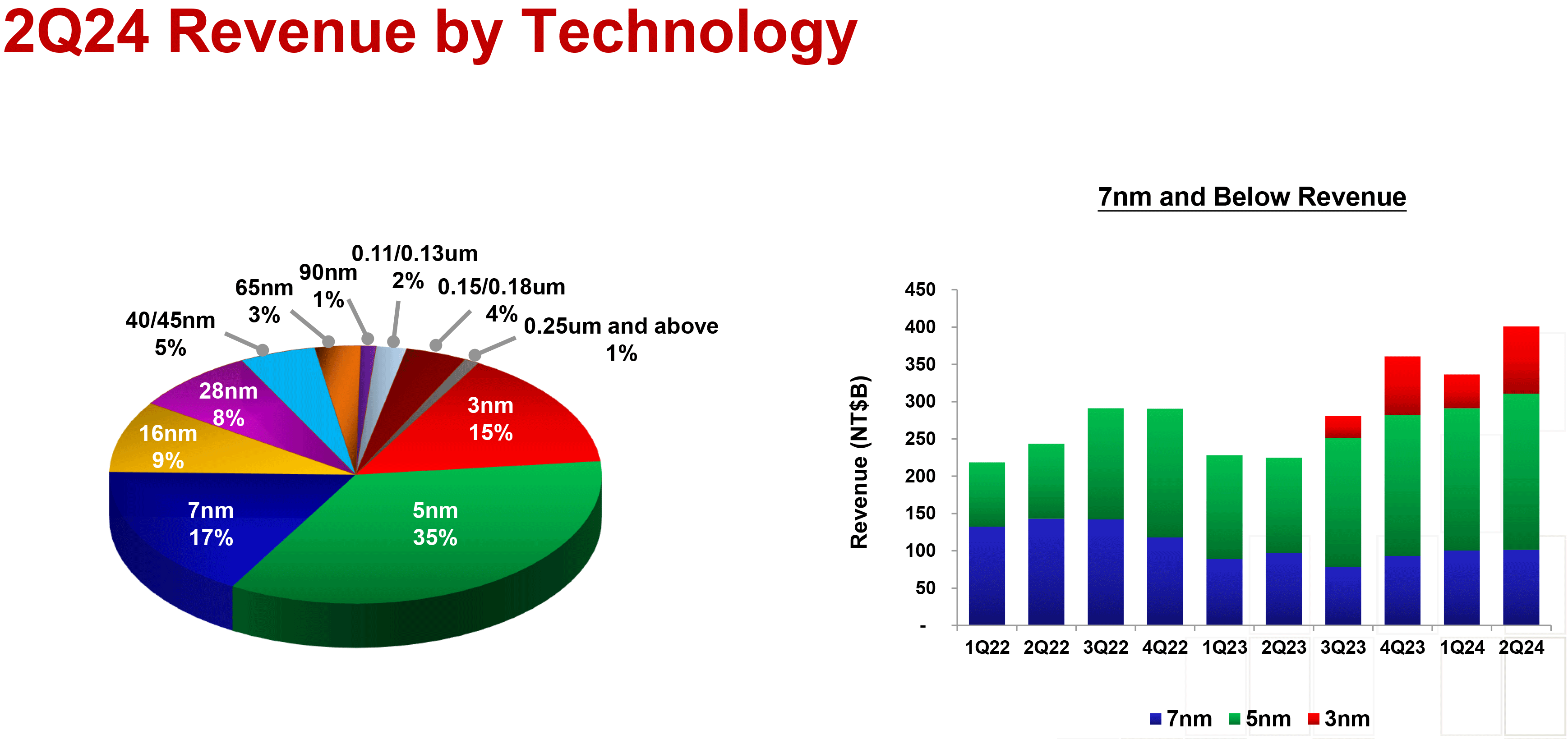
When it comes to wafer revenue share, the company's N3 process technologies (3nm-class) accounted for 15% of wafer revenue in Q2 (up from 9% in the previous quarter), N5 production nodes (4nm and 5nm-classes) commanded 35% of TSMC's earnings in the second quarter (down from 37% in Q1 2024), and N7 fabrication processes (6nm and 7nm-classes) accounted for 17% of the foundry's wafer revenue in the second quarter of 2024 (down from 19% in Q1 2024). Advanced technologies all together (N3, N5, N7) accounted for 67% of total wafer revenue.
"Our business in the second quarter was supported by strong demand for our industry-leading 3nm and 5nm technologies, partially offset by continued smartphone seasonality," said Wendell Huang, Senior VP and Chief Financial Officer of TSMC. "Moving into third quarter 2024, we expect our business to be supported by strong smartphone and AI-related demand for our leading-edge process technologies."
TSMC usually starts ramping up production for Apple's fall products (e.g. iPhone) in the second quarter of the year, so it is not surprising that revenue share of N3 increased in Q2 of this year. Yet, keeping in mind that TSMC's revenue in general increased by 10.3% QoQ, the company's shipments of processors made on N5 and N7 nodes are showing resilience as demand for AI and HPC processors is high across the industry.
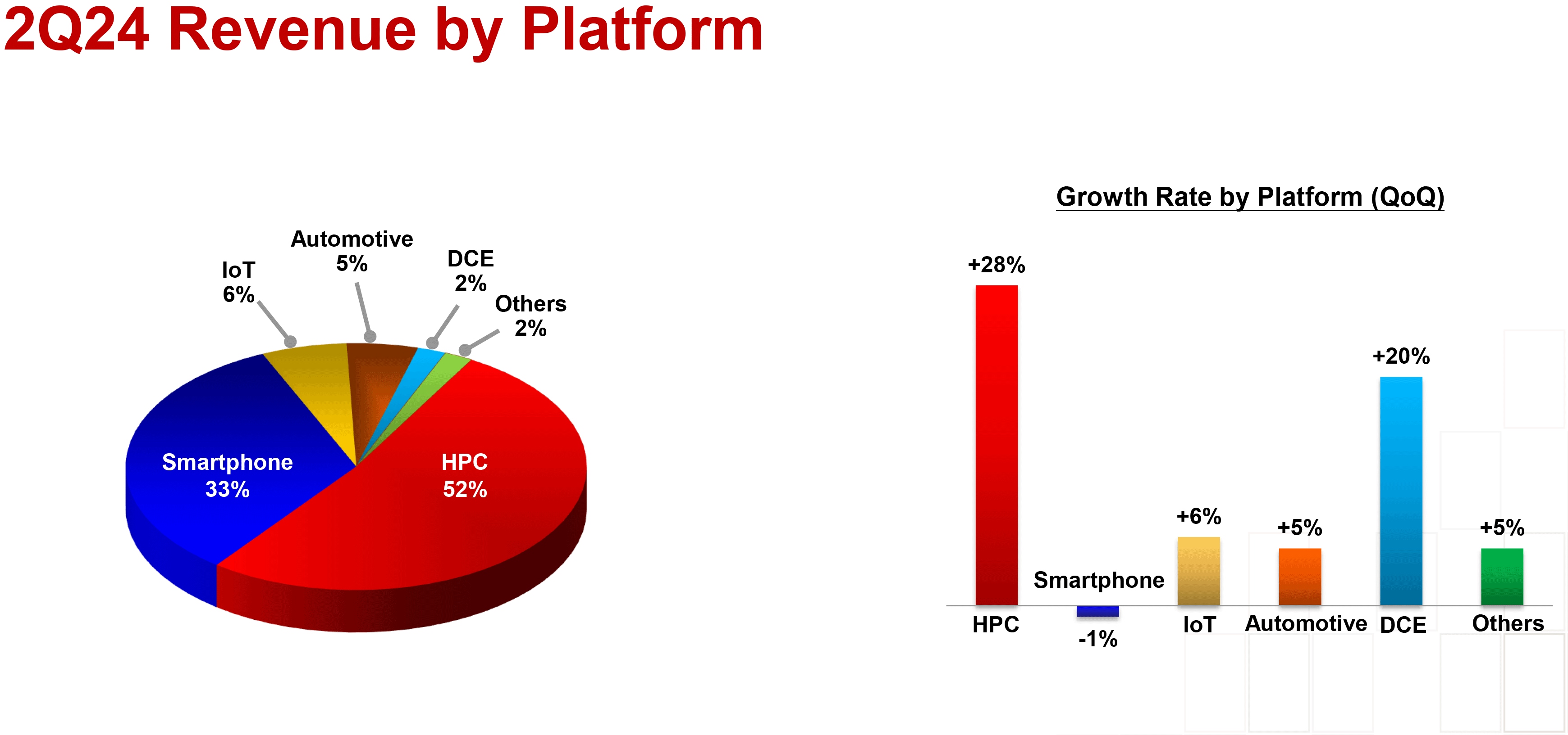
Speaking of TSMC's HPC sales, HPC platform sales accounted for 52% of TSMC's revenue for the first time in many years. The world's largest contract maker of chips produces many types of chips that get placed under the HPC umbrella, including AI processors, CPUs for client PCs, and system-on-chips (SoCs) for consoles, just to name a few. Yet, in this case TSMC attributes demand for AI processors as the main driver for its HPC success.
As for smartphone platform revenue, its share dropped to 33% as actual sales declined by 1% quarter-over-quarter. All other segments grew by 5% to 20%.
For the third quarter of 2024, TSMC expects revenue between US$22.4 billion and US$23.2 billion, with a gross profit margin of 53.5% to 55.5% and an operating profit margin of 42.5% to 44.5%. The company's sales are projected to be driven by strong demand for leading-edge process technologies as well as increased demand for AI and smartphones-related applications.
The Corsair RM750e ATX 3.1 Review: Simple And Effective
Published: Jul 18nd 2024 9:00am on AnandTech
As mainstream power supplies continue to make their subtle shift to the ATX 3.1 standard, the pace of change is picking up. Already most vendors offer at least one ATX 3.1 unit in their lineups, and thanks to the relatively small set of changes that come with the revised standard, PSU vendors have largely been able to tweak their existing ATX 3.0 designs, allowing for them to quickly roll-out updated power supplies. This means that the inflection point for ATX 3.1 as a whole is quickly approaching, as more and more designs get their update and make their way out to retail shelves.
Today we're looking at our first ATX 3.1-compliant PSU from Corsair, one of the industry's most prolific (and highest profile) power supply vendors. Their revised RMe line of power supplies are aimed at the mainstream gaming market, which is perhaps not too surprising given how important ATX 3.1 support and safety are to video cards. The RM750e model we're looking at today is the smallest capacity for the lineup, which stretches from 750 Watts up to a hefty 1200 Watts.
Overall, the RM750e is built to meet the demands of contemporary gaming systems, and boasts a great balance between features, performance, and cost. It is an 80Plus Gold certified unit with modular cables and PCIe 5.1/ATX 3.1 certified, offering a single 600W 12V-2x6 connector. We will explore its specifications, construction, and performance to determine its standing in today’s market.
Crucial P310 NVMe SSD Unveiled: Micron's Play in the M.2 2230 Market
Published: Jul 17nd 2024 9:00am on AnandTech
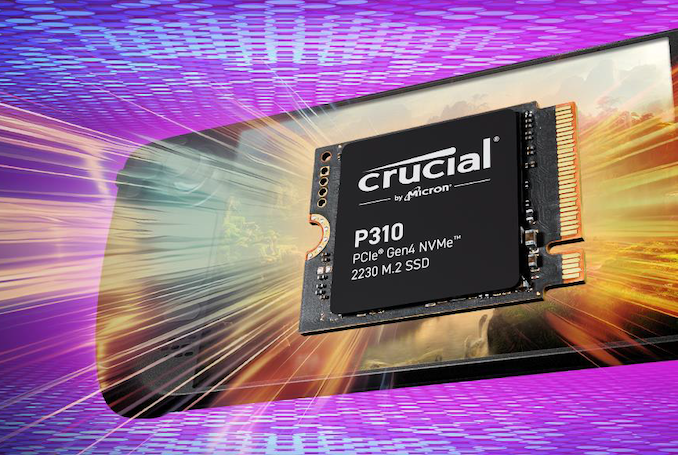
Hand-held gaming consoles based on notebook platforms (such as the Valve SteamDeck, ASUS ROG Ally, and the MSI Claw) are one of the fastest growing segments in the PC gaming market. The form-factor of such systems has created a demand for M.2 2230 NVMe SSDs. Almost all vendors have a play in this market, and even Micron has OEM SSDs (such as the Micron 2400, 2550, and 2500 series) in this form-factor. Crucial has strangely not had an offering with its own brand name to target this segment, but that changes today with the launch of the Crucial P310 NVMe SSD.
The Crucial P310 is a family of M.2 2230 PCIe Gen4 NVMe SSDs boasting class-leading read/write speeds of 7.1 GBps and 6 GBps. The family currently has two capacity points - 1 TB and 2 TB. Micron claims that the use of its 232L 3D NAND and Phison's latest E27T DRAM-less controller (fabricated in TSMC's 12nm process) help in reducing power consumption under active use compared to the competition - directly translating to better battery life for the primary use-case involving gaming handheld consoles.
Based on the specifications, it appears that the drives are using 232L 3D QLC, and we have reached out to Micron to confirm the same. Compared to the recently-released Micron 2550 SSD series in the same form-factor, a swap in the controller has enabled some improvements in both power efficiency and performance. The other specifications are summarized in the table below.
Crucial P310 SSD Specifications Capacity 2 TB 1 TB Controller Phison E27T (DRAM-less) NAND Flash Micron 232L 3D NAND (QLC?) Form-Factor, Interface Single-Sided M.2-2230 PCIe 4.0 x4, NVMe Sequential Read 7100 MB/s Sequential Write 6000 MB/s Random Read IOPS 1 M Random Write IOPS 1.2 M SLC Caching Yes TCG Pyrite Encryption Yes Warranty 5 Years Write Endurance 440 TBW 0.12 DWPD 220 TBW 0.12 DWPD MSRP $215 $115The power efficiency, cost, and capacity points are plus points for the Crucial P310 family. However, the endurance ratings are quite low. Gaming workloads are inherently read-heavy, and this may not be a concern for the average consumer. However, a 0.12 DWPD rating may turn out to be a negative aspect when compared against the competition's 0.33 DWPD offerings in the same segment.
Samsung Validates LPDDR5X Running at 10.7 GT/sec with MediaTek's Dimensity 9400 SoC
Published: Jul 17nd 2024 8:00am on AnandTech
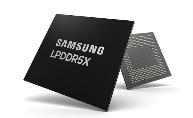
Samsung has successfully validated its new LPDDR5X-10700 memory with MediaTek's upcoming Dimensity platform. At present, 10.7 GT/s is the highest performing speed grade of LPDDR5X DRAM slated to be released this year, so the upcoming Dimensity 9400 system-on-chip will get the highest memory bandwidth available for a mobile application processor.
The verification process involved Samsung's 16 GB LPDDR5X package and MediaTek's soon-to-be-announced Dimensity 9400 SoC for high-end 5G smartphones. Usage of LPDDR5X-10700 provides a memory bandwidth of 85.6 GB/second over a 64-bit interface, which will be available for bandwidth-hungry applications like graphics and generative AI.
"Working together with Samsung Electronics has made it possible for MediaTek's next-generation Dimensity chipset to become the world's first to be validated at LPDDR5X operating speeds up to 10.7Gbps, enabling upcoming devices to deliver AI functionality and mobile performance at a level we have never seen before," said JC Hsu, Corporate Senior Vice President at MediaTek. "This updated architecture will make it easier for developers and users to leverage more AI capabilities and take advantage of more features with less impact on battery life."
Samsung's LPDDR5X 10.7 GT/s memory in made on the company's 12nm-class DRAM process technology and is said to provide a more than 25% improvement in power efficiency over previous-generation LPDDR5X, in addition to extra performance. This will positively affect improved user experience, including enhanced on-device AI capabilities, such as faster voice-to-text conversion, and better quality graphics.
Overall, the two companies completed this process in just three months. Though it remains to be seen when smartphones based on the Dimensity 9400 application processor and LPDDR5X memory are set to be available on the market, as MediaTek has not yet even formally announced the SoC itself.
"Through our strategic cooperation with MediaTek, Samsung has verified the industry's fastest LPDDR5X DRAM that is poised to lead the AI smartphone market," said YongCheol Bae, Executive Vice President of Memory Product Planning at Samsung Electronics. "Samsung will continue to innovate through active collaboration with customers and provide optimum solutions for the on-device AI era."
Western Digital Adds 8 TB Version of Popular High-End SN850X SSD
Published: Jul 16nd 2024 5:30am on AnandTech
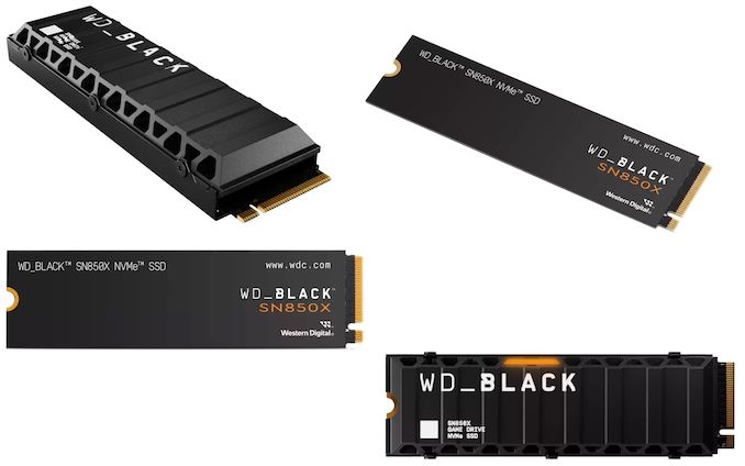
Western Digital has quietly introduced an 8 TB version of its high-end SN850X SSD, doubling the top capacity of the well-regarded drive family. The new drive offers performance on par with other members of the range, but with twice as much capacity as the previous top-end model – and with a sizable price premium to go with its newfound capacity.
Western Digital introduced its WD_Black SN850X SSDs in the summer of 2022, releasing single-sided 1 TB and 2 TB models, along with a double-sided 4 TB model. But now almost two years down the line, the company has seen it fit to introduce the even higher capacity 8 TB model to serve as their flagship PCIe 4.0 SSD, and keep with the times of NAND prices and SSD capacity demands.
Like the other SN850X models, WD is using their in-house, 4-channel controller for the new 8 TB model, which sports a PCIe 4.0 x4 interface. And being that this is a high-end SSD, the controller is paired with DRAM (DDR4) for page index caching, though WD doesn't disclose how much DRAM is on any given model. On the NAND front, WD is apparently still using their BiCS 5 112L NAND here, which means we're looking at 4x 2 TB NAND chips, each with 16 1Tbit TLC dies on-board, twice as many dies as were used on the NAND chips for the 4 TB model.
The peak read speed of the new 8TB model is 7,200 MB/sec, which is actually a smidge below the performance the 4 TB and 2 TB models due to the overhead from the additional NAND dies. Meanwhile peak sequential write speeds remain at 6,600 MB/sec, while 4K random write performance maxes out at 1200K IOPS for both reads and writes. It goes without saying that this is a step below the performance of the market flagship PCIe 5.0 SSDs available today, but it's going to be a bit longer until anyone else besides Phison is shipping a PCIe 5.0 controller – never mind the fact that these drives aren't available in 8 TB capacities.
The 8 TB SN850X also keeps the same drive endurance progression as the rest of the SN850X family. In this case, double the NAND brings double the endurance of the 4 TB model, for an overall endurance of 4800 terabytes written (TBW). Or in terms of drive writes per day, this is the same 0.33 rating as the other SN850X drives.
WD_Back SN850X SSD Specifications Capacity 8 TB 4 TB 2 TB 1 TB Controller WD In-House: 4 Channel, DRAM (DDR4) NAND Flash WD BiCS 5 TLC Form-Factor, Interface Double-Sided M.2-2280 PCIe 4.0 x4, NVMe Single-Sided M.2-2280 PCIe 4.0 x4, NVMe Sequential Read 7200 MB/s 7300 MB/s 7300 MB/s 7300 MB/s Sequential Write 6600 MB/s 6600 MB/s 6600 MB/s 6300 MB/s Random Read IOPS 1200K 1200K 1200K 800K Random Write IOPS 1200K 1100K 1100K 1100K SLC Caching Yes TCG Opal Encryption 2.01 Warranty 5 Years Write Endurance 4800 TBW 0.33 DWPD 2400 TBW 0.33 DWPD 1200 TBW 0.33 DWPD 600 TBW 0.33 DWPD MSRP (No Heatsink) $850 $260 $140 $85Western Digital's WD_Black SN850X is available both with and without aluminum heatsink. The version without a heatsink aimed at laptops and BYOC setups costs $849.99, whereas a version with an aluminum heat spreader comes at $899.99. In both cases the 8 TB drive carries a significant price premium over the existing 4 TB model, which is readily available for $259.99.
This kind of price premium is unfortunately typical for 8 TB drives, and will likely remain so until both supply and demand for the high-capacity drives picks up to bring prices down. Still, with rival drives such as Corsair's MP600 Pro XT 8 TB and Sabrent's Rocket 4 Plus 8 TB going for $965.99 and $1,199.90 respectively, the introduction of the 8 TB SN850X is definitely pushing high-capacity M.2 SSD prices down, albeit slowly. So for systems with multiple M.2 slots, at least, the sweet spot on drive pricing is still to get two 4 TB SSDs.
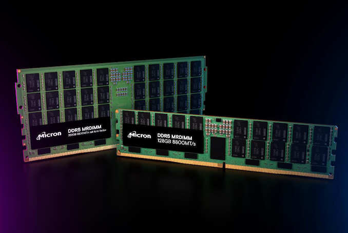
Micron Expands Datacenter DRAM Portfolio with MR-DIMMs
Published: Jul 16nd 2024 9:10am on AnandTech
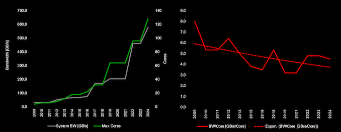
The compute market has always been hungry for memory bandwidth, particularly for high-performance applications in servers and datacenters. In recent years, the explosion in core counts per socket has further accentuated this need. Despite progress in DDR speeds, the available bandwidth per core has unfortunately not seen a corresponding scaling.
The stakeholders in the industry have been attempting to address this by building additional technology on top of existing widely-adopted memory standards. With DDR5, there are currently two technologies attempting to increase the peak bandwidth beyond the official speeds. In late 2022, SK hynix introduced MCR-DIMMs meant for operating with specific Intel server platforms. On the other hand, JEDEC - the standards-setting body - also developed specifications for MR-DIMMs with a similar approach. Both of them build upon existing DDR5 technologies by attempting to combine multiple ranks to improve peak bandwidth and latency.
How MR-DIMMs WorkThe MR-DIMM standard is conceptually simple - there are multiple ranks of memory modules operating at standard DDR5 speeds with a data buffer in front. The buffer operates at 2x the speed on the host interface side, allowing for essentially double the transfer rates. The challenges obviously lie in being able to operate the logic in the host memory controller at the higher speed and keeping the power consumption / thermals in check.
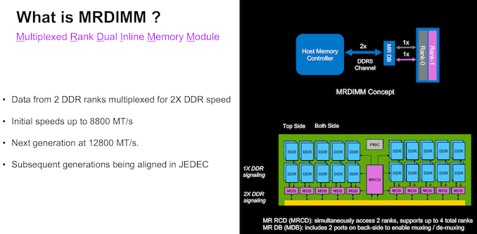
The first version of the JEDEC MR-DIMM standard specifies speeds of 8800 MT/s, with the next generation at 12800 MT/s. JEDEC also has a clear roadmap for this technology, keeping it in sync with the the improvements in the DDR5 standard.
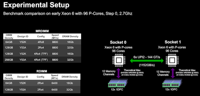
Micron MR-DIMMs - Bandwidth and Capacity PlaysMicron and Intel have been working closely in the last few quarters to bring their former's first-generation MR-DIMM lineup to the market. Intel's Xeon 6 Family with P-Cores (Granite Rapids) is the first platform to bring MR-DIMM support at 8800 MT/s on the host side. Micron's standard-sized MR-DIMMs (suitable for 1U servers) and TFF (tall form-factor) MR-DIMMs (for 2U+ servers) have been qualified for use with the same.
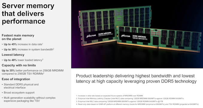
The benefits offered by MR-DIMMs are evident from the JEDEC specifications, allowing for increased data rates and system bandwidth, with improvements in latency. On the capacity side, allowing for additional ranks on the modules has enabled Micron to offer a 256 GB capacity point. It must be noted that some vendors are also using TSV (through-silicon vias) technology to to increase the per-package capacity at standard DDR5 speeds, but this adds additional cost and complexity that are largely absent in the MR-DIMM manufacturing process.
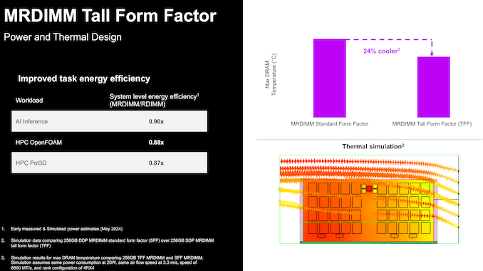
The tall form-factor (TFF) MR-DIMMs have a larger surface area compared to the standard-sized ones. For the same airflow configuration, this allows the DIMM to have a better thermal profile. This provides benefits for energy efficiency as well by reducing the possibility of thermal throttling.
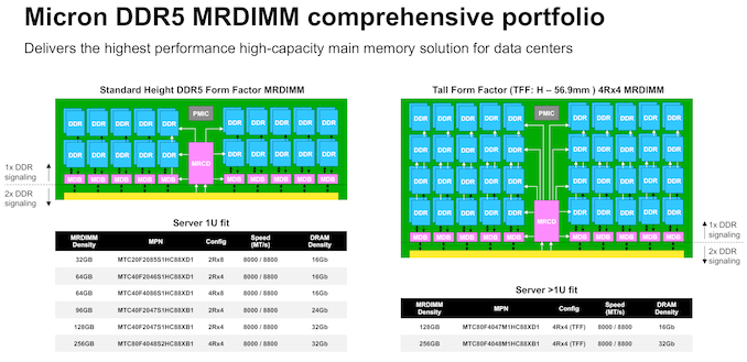
Micron is launching a comprehensive lineup of MR-DIMMs in both standard and tall form-factors today, with multiple DRAM densities and speed options as noted above.
MRDIMM Benefits - Intel Granite Rapids Gets a Performance BoostMicron and Intel hosted a media / analyst briefing recently to demonstrate the benefits of MR-DIMMs for Xeon 6 with P-Cores (Granite Rapids). Using a 2P configuration with 96-core Xeon 6 processors, benchmarks for different workloads were processed with both 8800 MT/s MR-DIMMs and 6400 MT/s RDIMMs. The chosen workloads are particularly notorious for being limited in performance by memory bandwidth.
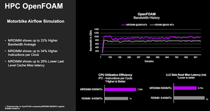
OpenFOAM is a widely-used CFD workload that benefits from MR-DIMMs. For the same memory capacity, the 8800 MT/s MR-DIMM shows a 1.31x speedup based on higher average bandwidth and IPC improvements, along with lower last-level cache miss latency.
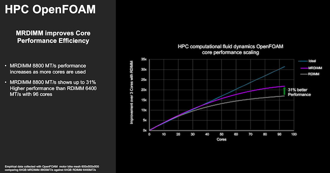
The performance benefits are particularly evident with more cores participating the workload.
Apache Spark is a commonly used big-data platform operating on large datasets. Depending on the exact dataset in the picture, the performance benefits of MR-DIMMs can vary. Micron and Intel used a 2.4TB set from Intel's Hibench benchmark suite for this benchmark, showing a 1.2x speedup at the same capacity and 1.7x speedup with doubled-capacity TFF MR-DIMMs.
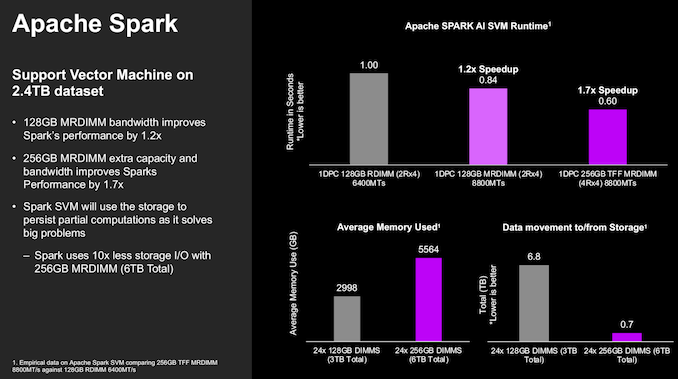
Avoiding the need to push data back to the permanent storage also contributes to the speedup.
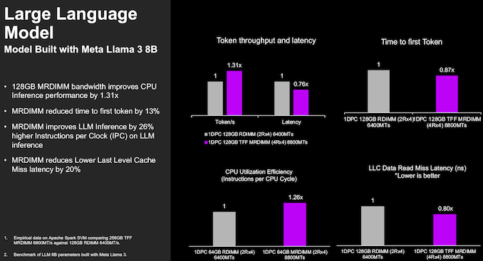
The higher speed offered by MR-DIMMs also helps in AI inferencing workloads, with Micron and Intel showing a 1.31x inference performance improvement along with reduced time to first token for a Llama 3 8B parameter model. Obviously, purpose-built inferencing solutions based on accelerators will perform better. However, this was offered as a demonstration of the type of CPU workloads that can benefit from MR-DIMMs.
As the adage goes, there is no free lunch. At 8800 MT/s, MR-DIMMs are definitely going to guzzle more power compared to 6400 MT/s RDIMMs. However, the faster completion of workloads mean that the the energy consumption for a given workload will be lower for the MR-DIMM configurations. We would have liked Micron and Intel to quantify this aspect for the benchmarks presented in the demonstration. Additionally, Micron indicated that the energy efficiency (in terms of pico-joules per bit transferred) is largely similar for both the 6400 MT/s RDIMMs and 8800 MT/s MR-DIMMs.
Key TakeawaysThe standardization of MR-DIMMs by JEDEC allows multiple industry stakeholders to participate in the market. Customers are not vendor-locked and can compare and contrast options from different vendors to choose the best fit for their needs.
At Computex, we saw MR-DIMMs from ADATA on display. As a Tier-2 vendor without its own DRAM fab, ADATA's play is on cost benefits with the possibility of the DRAM die being sourced from different fabs. The MR-DIMM board layout is dictated by JEDEC specifications, and this allows Tier-2 vendors to have their own play with pricing flexibility. Modules are also built based on customer orders. Micron, on the other hand, has a more comprehensive portfolio / lineup of SKUs for different use-cases with the pros and cons of vertical integration in the picture.
Micron is also not the first to publicly announce MR-DIMM sampling. Samsung announced their own lineup (based on 16Gb DRAM dies) last month. It must be noted that Micron's MR-DIMM portfolio uses 16 Gb, 24 Gb, and 32 Gb dies fabricated in 1β technology. While Samsung's process for the 16 Gb dies used in their MR-DIMMs is not known, Micron believes that their MR-DIMM technology will provide better power efficiency compared to the competition while also offering customers a wider range of capacities and configurations.
The AMD Zen 5 Microarcitecure: Powering Ryzen AI 300 Series For Mobile and Ryzen 9000 for Desktop
Published: Jul 15nd 2024 9:00am on AnandTech
Back at Computex 2024, AMD unveiled their highly anticipated Zen 5 CPU microarchitecture during AMD CEO Dr. Lisa Su's opening keynote. AMD announced not one but two new client platforms that will utilize the latest Zen 5 cores. This includes AMD's latest AI PC-focused chip family for the laptop market, the Ryzen AI 300 series. In comparison, the Ryzen 9000 series caters to the desktop market, which uses the preexisting AM5 platform.
Built around the new Zen 5 CPU microarchitecture with some fundamental improvements to both graphics and AI performance, the Ryzen AI 300 series, code-named Strix Point, is set to deliver improvements in several areas. The Ryzen AI 300 series looks set to add another footnote in the march towards the AI PC with its mobile SoC featuring a new XDNA 2 NPU, from which AMD promises 50 TOPS of performance. AMD has also upgraded the integrated graphics with the RDNA 3.5, which is designed to replace the last generation of RDNA 3 mobile graphics, for better performance in games than we've seen before.
Further to this, during AMD's recent Tech Day last week, AMD disclosed some of the technical details regarding Zen 5, which also covers a number of key elements under the hood on both the Ryzen AI 300 and the Ryzen 9000 series. On paper, the Zen 5 architecture looks quite a big step up compared to Zen 4, with the key component driving Zen 5 forward through higher instructions per cycle than its predecessor, which is something AMD has managed to do consistently from Zen to Zen 2, Zen 3, Zen 4, and now Zen 5.
Troubled AI Processor Developer Graphcore Finds a Buyer: SoftBank
Published: Jul 12nd 2024 4:30am on AnandTech
After months of searching for a buyer, troubled U.K.-based AI processor designer Graphcore said on Friday that it has been acquired by SoftBank. The company will operate as a wholly owned subsidiary of SoftBank and will possibly collaborate with Arm, but what remains to be seen what happens to the unique architecture of Graphcore's intelligence processing units (IPUs).
Graphcore will retain its name as it will become a wholly owned subsidiary of SoftBank, which paid either $400 million (according to EE Times) or $500 million (according to BBC) for the company. Over its lifetime, Graphcore has received a total of $700 million of investments from Microsoft and Sequoia Capital, and at its peak in late 2020, was valued at $2.8 billion. Nigel Toon will remain at the helm of Graphcore, which will hire new staff in its UK offices and continue to be headquartered in Bristol, with additional offices in Cambridge, London, Gdansk (Poland), and Hsinchu (China).
"This is a tremendous endorsement of our team and their ability to build truly transformative AI technologies at scale, as well as a great outcome for our company," said Nigel Toon. "Demand for AI compute is vast and continues to grow. There remains much to do to improve efficiency, resilience, and computational power to unlock the full potential of AI. In SoftBank, we have a partner that can enable the Graphcore team to redefine the landscape for AI technology."
Although Graphcore says that it had won contracts with major high-tech companies and deployed its IPUs, it could not compete against NVIDIA and other prêt-à-porter AI processor vendors due to insufficient funding. In the recent years the company's problems were so severe that it had to lay off 20% of its staff, bringing its headcount to around 500. Those cuts also saw office closures in Norway, Japan, and South Korea, which made it even harder to compete against big players.
Graphcore certainly hopes that with SoftBank's deep pockets and willingness to invest in AI technologies in general and AI processors in particular, it will finally be able to compete head-to-head with established players like NVIDIA.
When asked whether Graphcore will work with SoftBank's Arm, Nigel Toon said that he was looking forward to work with all companies controlled by its parent, including Arm. Meanwhile, SoftBank itself is reportedly looking forward to build its own AI processor venture called Project Izanagi to compete against NVIDIA, whereas Arm is reportedly developing AI processors that will work in datacenters owned by SoftBank. Therefore, it remains to be seen where does Graphcore fit in.
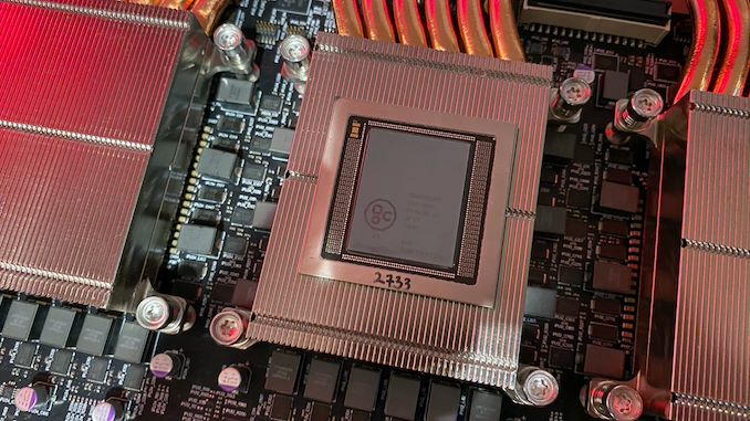
For now, the best processor that Graphcore has is its Colossus MK2 IPU, which is built using 59.4 billion transistors and packs in 1,472 independent cores with simultaneous multithreading (SMT) capable of handling 8,832 parallel threads. Instead of using HBM or other types of external memory, the chip integrates 900 MB of SRAM, providing an aggregated bandwidth of 47.5 TB/s per chip. Additionally, it features 10 IPU links to scale with other MK2 processors. When it comes to performance, the MK2 C600 delivers 560 TFLOPS FP8, 280 TFLOPS FP16, and 70 TFLOPS of FP32 performance at 185W. To put the numbers into context, NVIDIA's A100 delivers 312 FP16 TFLOPS without sparsity as well as 19.5 FP32 TFLOPS, whereas NVIDIA's H100 card offers 3,341 FP8 TFLOPS.
Applied Materials' New Deposition Tool Enables Copper Wires to Be Used for 2nm and Beyond
Published: Jul 12nd 2024 8:00am on AnandTech
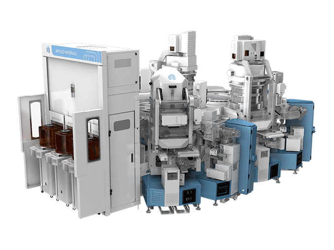
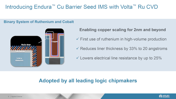
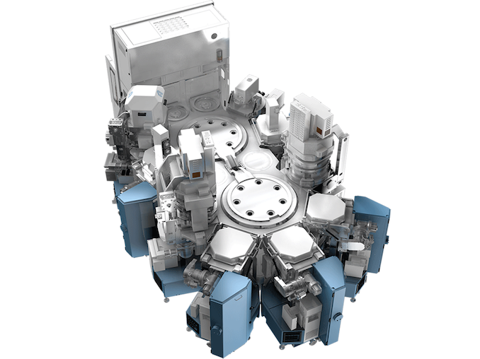
Although the pace of Moore's Law has undeniably slackened in the last decade, transistor density is still increasing with every new process technology. But there is a challenge with feeding power to smaller transistors, as with the smaller transistors comes thinner power wires within the chip, which increases their resistance and may cause yield loss. Looking to combat that effect, this week Applied Materials introduced its new Applied Endura Copper Barrier Seed IMS with Volta Ruthenium Copper Vapor Deposition (CVD) tool, which enables chipmakers to keep using copper for wiring with 2 nm-class and more advanced process technologies.
Today's advanced logic processors have about 20 layers of metal, with thin signal wires and thicker power wires. Scaling down wiring with shrinking transistors presents numerous challenges. Thinner wires have higher electrical resistance, while closer wires heighten capacitance and electrical crosstalk. The combination of the two can lead to increased power consumption while also limiting performance scaling, which is particularly problematic for datacenter grade processors that are looking to have it all. Moving power rails to a wafer's back-side is expected to enhance performance and efficiency by reducing wiring complexity and freeing up space for more transistors.
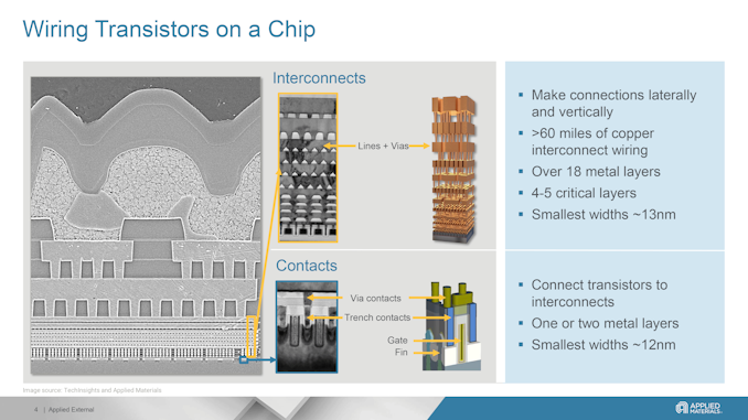
But backside power delivery network (BSPDN) does not solve the problem with thin wires in general. As lithographic scaling progresses, both transistor features and wiring trenches become smaller. This reduction means that barriers and liners take up more space in these trenches, leaving insufficient room to deposit copper without creating voids, which raises resistance and can lower yields. Additionally, the closer proximity of wires thins the low-k dielectrics, making them more vulnerable to damage during the etching process. This damage increases capacitance and weakens the chips, making them unsuitable for 3D stacking. Consequently, as the industry advances, copper wiring faces significant physical scaling challenges. But Applied Materials has a solution.
Adopting Binary RuCo LinersContemporary manufacturing technologies use reflow to fill interconnects with copper, where anneals help the copper flow from the wafer surface into wiring trenches and vias. This process depends on the liners on which the copper flows. Normally, a CVD cobalt film was used for liners, but this film is too thick for 3nm-class nodes (which would affect resistance and yield).
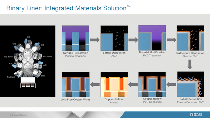
Applied Materials proposes using a ruthenium cobalt (RuCo) binary liner with a thickness under 20A (2nm, 20 angstroms), which would provide better surface properties for copper reflow. This would ultimately allow for 33% more space for void-free conductive copper to be reflowed, reducing the overall resistance by 25%. While usage of the new liner requires new tooling, it can enable better interconnects that mean higher performance, lower power consumption and higher yields.
Gallery: Applied Materials New Tool Enables Copper Wires to Be Used for 2nm and Beyond


Applied Materials says that so far its new Endura Copper Barrier Seed IMS with Volta Ruthenium CVD tool has been adopted by all leading logic makers, including TSMC and Samsung Foundry for their 3nm-class nodes and beyond.
"The semiconductor industry must deliver dramatic improvements in energy-efficient performance to enable sustainable growth in AI computing," said Dr. Y.J. Mii, Executive Vice President and Co-Chief Operating Officer at TSMC. "New materials that reduce interconnect resistance will play an important role in the semiconductor industry, alongside other innovations to improve overall system performance and power."
New Low-K DielectricBut thin and efficient liner is not the only thing crucial for wiring at 3nm production nodes and beyond. Trenches for wiring are filed not only with a Co/RuCo liner and a Ta/N barrier, but with low dielectric constant (Low-K) film to minimize electrical charge buildup, reduce power consumption, and lower signal interference. Applied Materials has offered its Black Diamond Low-K film since the early 2000s.
But new production nodes require better dielectrics, so this week the company introduced an upgraded version of Black Diamond material and a plasma-enhanced chemical vapor deposition (PEVCD) tool to apply it, the Producer Black Diamond PECVD series. This new material allows for scaling down to 2nm and beyond by further reducing the dielectric constant while also increasing the mechanical strength of the chips, which is good for 3D stacking both for logic and memory. The new Black Diamond is being rapidly adopted by major logic and DRAM chipmakers, Applied says.
"The AI era needs more energy-efficient computing, and chip wiring and stacking are critical to performance and power consumption," said Dr. Prabu Raja, President of the Semiconductor Products Group at Applied Materials. "Applied's newest integrated materials solution enables the industry to scale low-resistance copper wiring to the emerging angstrom nodes, while our latest low-k dielectric material simultaneously reduces capacitance and strengthens chips to take 3D stacking to new heights."
Samsung Joins The 60 TB SSD Club, Looking Forward To 120 TB Drives
Published: Jul 5nd 2024 11:00am on AnandTech
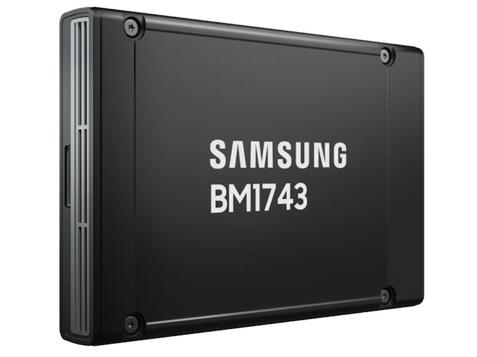
Multiple companies offer high-capacity SSDs, but until recently, only two companies offered high-performance 60 TB-class drives with a PCIe interface: Solidigm and Western Digital. As our colleagues from Blocks & Files discovered, Samsung quietly rolled out its BM1743 61.44 TB solid-state drive in mid-June and now envisions 120 TB-class SSDs based on the same platform.
Samsung's BM1743 61.44 TB features a proprietary controller and relies on Samsung's 7th Generation V-NAND (3D NAND) QLC memory. Moreover, Samsung believes that its 7th Gen V-NAND 'has the potential to accommodate up to 122.88 TB,'
Samsung plans to offer the BM1743 in two form factors: U.2 for PCIe 4.0 x4 to address traditional servers and E3.S for PCIe 5.0 x4 interfaces to address machines designed to offer maximum storage density. BM1743 can address various applications, including AI training and inference, content delivery networks, and read-intensive workloads. To that end, its write endurance is 0.26 drive writes per day (DWPD) over five years.
Regarding performance, Samsung's BM1743 is hardly a champion compared to high-end drives for gaming machines and workstations. The drive can sustainably achieve sequential read speeds of 7,200 MB/s and write speeds of 2,000 MB/s. It can handle up to 1.6 million 4K random reads and 110,000 4K random writes for random operations.
Power consumption details for the BM1743 have not been disclosed, though it is expected to be high. Meanwhile, the drive's key selling point is its massive storage density, which likely outweighs concerns over its absolute power efficiency for intended applications, as a 60 TB SSD still consumes less than multiple storage devices offering similar capacity and performance.
As noted above, Samsung's BM1743 61.44 TB faces limited competition in the market, so its price will be quite high. For example, Solidigm's D5-P5336 61.44 TB SSD costs $6,905. Other companies, such as Kioxia, Micron, and SK Hynix, have not yet introduced their 60TB-class SSDs, which gives Samsung and Solidigm an edge for now.