Intel to Launch "Lunar Lake" Core Ultra Chips on September 3rd
Published: Jul 31nd 2024 8:00am on AnandTech
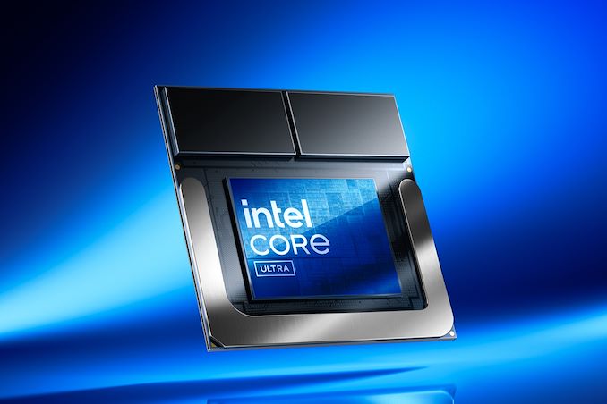
Intel’s next-generation Core Ultra laptop chips finally have a launch date: September 3rd.
Codenamed Lunar Lake, Intel has been touting the chips for nearly a year now. Most recently, Intel offered the press a deep dive briefing on the chips and their underlying architectures at Computex back in June, along with a public preview during the company’s Computex keynote. At the time Intel was preparing for Q3’2024 launch, and that window has finally been narrowed down to a single date – September 3rd – when Intel will be hosting their Lunar Lake launch event ahead of IFA.
Intel’s second stab at a high volume chiplet-based processor for laptop users, Lunar Lake is aimed particularly at ultrabooks and other low-power mobile devices, with Intel looking to wrestle back the title of the most efficient PC laptop SoC. Lunar Lake is significant in this respect as Intel has never previously developed a whole chip architecture specifically for low power mobile devices before – it’s always been a scaled-down version of a wider-range architecture, such as the current Meteor Lake (Core Ultra 100 series). Consequently, Intel has been touting that they’ve make some serious efficiency advancements with their highly targeted chip, which they believe will vault them over the competition.
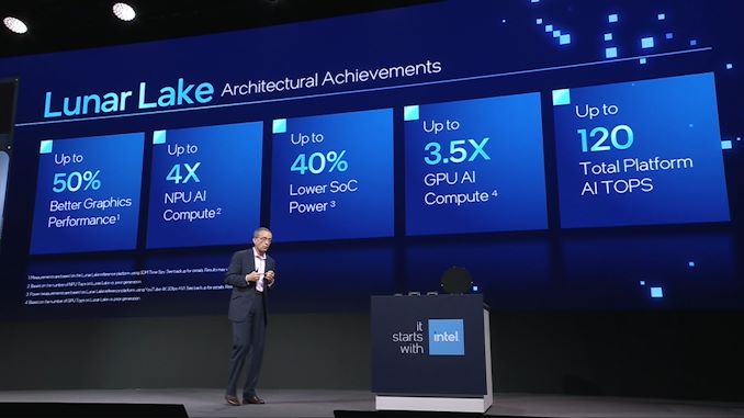
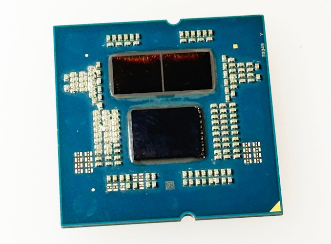
All told, Lunar Lake is slated to bring a significant series of updates to Intel’s chip architectures and chip design strategies. Of particular interest is the switch to on-package LPDDR5X memory, which is a first for a high-volume Core chip. As well, Lunar Lake incorporates updated versions of virtually every one of Intel’s architecture, from the CPU P and E cores – Lion Cove and Skymont respectively – to the Xe2 GPU and 4th generation NPU (aptly named NPU 4). And, in a scandalous twist, both of the chiplets/tiles on the CPU are being made by TSMC. Intel isn’t providing any of the active silicon for the chip – though they are providing the Foveros packaging needed to put it together.
Intel CPU Architecture Generations Alder/Raptor Lake Meteor Lake Lunar Lake Arrow Lake Panther Lake P-Core Architecture Golden Cove/ Raptor Cove Redwood Cove Lion Cove Lion Cove Cougar Cove? E-Core Architecture Gracemont Crestmont Skymont Crestmont? Darkmont? GPU Architecture Xe-LP Xe-LPG Xe2 Xe2? ? NPU Architecture N/A NPU 3720 NPU 4 ? ? Active Tiles 1 (Monolithic) 4 2 4? ? Manufacturing Processes Intel 7 Intel 4 + TSMC N6 + TSMC N5 TSMC N3B + TSMC N6 Intel 20A + More Intel 18A Segment Mobile + Desktop Mobile LP Mobile HP Mobile + Desktop Mobile? Release Date (OEM) Q4'2021 Q4'2023 Q3'2024 Q4'2024 2025Suffice it to say, no matter what happens, Lunar Lake and the Core Ultra 200 series should prove to be an interesting launch.
It’s worth noting, however, that while Intel’s announcement of their livestreamed event is being labeled a “launch event” by the company, the brief reveal doesn’t make any claims about on-the-shelves availability. September 3rd is a Tuesday (and the day after a US holiday), which isn’t a typical launch date for new laptops (for reference, the lightly stocked Meteor Lake launch was a Thursday). So Intel’s launch event may prove to be more of a soft launch for Lunar Lake; we’ll have to see how things pan out in the coming weeks.
Gallery: Intel to Launch "Lunar Lake" Core Ultra Chips on September 3rd

The AMD Ryzen AI 9 HX 370 Review: Unleashing Zen 5 and RDNA 3.5 Into Notebooks
Published: Jul 28nd 2024 9:00am on AnandTech
During the opening keynote delivered by AMD CEO Dr. Lisa Su at Computex 2024, AMD finally lifted the lid on their highly-anticipated Zen 5 microarchitecture. The backbone for the next couple of years of everything CPU at AMD, the company unveiled their plans to bring Zen 5 in the consumer market, announcing both their next-generation mobile and desktop products at the same time. With a tight schedule that will see both platforms launch within weeks of each other, today AMD is taking their first step with the launch of the Ryzen AI 300 series – codenamed Strix Point – their new Zen 5-powered mobile SoC.
The latest and greatest from AMD, the Strix Point brings significant architectural improvements across AMD's entire IP portfolio. Headlining the chip, of course, is the company's new Zen 5 CPU microarchitecture, which is taking multiple steps to improve on CPU performance without the benefits of big clockspeed gains. And reflecting the industry's current heavy emphasis on AI performance, Strix Point also includes the latest XDNA 2-based NPU, which boasts up to 50 TOPS of performance. Other improvements include an upgraded integrated graphics processor, with AMD moving to the RDNA 3.5 graphics architecture.
The architectural updates in Strix Point are also seeing AMD opt for a heterogenous CPU design from the very start, incorporating both performance and efficiency cores as a means of offering better overall performance in power-constrained devices. AMD first introduced their compact Zen cores in the middle of the Zen 4 generation, and while they made it into products such as AMD's small-die Phoenix 2 platform, this is the first time AMD's flagship mobile silicon has included them as well. And while this change is going to be transparent from a user perspective, under the hood it represents an important improvement in CPU design. As a result, all Ryzen AI 300 chips are going to include a mix of not only AMD's (mostly) full-fat Zen 5 CPU cores, but also their compact Zen 5c cores, boosting the chips' total CPU core counts and performance in multi-threaded situations.
For today's launch, the AMD Ryzen AI 300 series will consist of just three SKUs: the flagship Ryzen AI 9 HX 375, with 12 CPU cores, as well as the Ryzen AI 9 HX 370 and Ryzen 9 365, with 12 and 10 cores respectively. All three SoCs combine both the regular Zen 5 core with the more compact Zen 5c cores to make up the CPU cluster, and are paired with a powerful Raden 890M/880M GPU, and a XDNA 2-based NPU.
As the successor to the Zen 4-based Phoenix/Hawk Point, the AMD Ryzen AI 300 series is targeting a diverse and active notebook market that has become the largest segment of the PC industry overall. And it is telling that, for the first time in the Zen era, AMD is launching their mobile chips first – if only by days – rather than their typical desktop-first launch. It's both a reflection on how the PC industry has changed over the years, and how AMD has continued to iterate and improve upon its mobile chips; this is as close to mobile-first as the company has ever been.
Getting down to business, for our review of the Ryzen AI 300 series, we are taking a look at ASUS's Zenbook S 16 (2024), a 16-inch laptop that's equipped with AMD's Ryzen AI 9 HX 370. The sightly more modest Ryzen features four Zen 5 CPU cores and 8 Zen 5c CPU cores, as well as AMD's latest RDNA 3.5 Radeon 890M integrated graphics. Overall, the HX 370 has a configurable TDP of between 15 and 54 W, depending on the desired notebook configuration.
Fleshing out the rest of the Zenbook S 16, ASUS has equipped the laptop with a bevy of features and technologies fitting for a flagship Ryzen notebook. The centerpiece of the laptop is a Lumina OLED 16-inch display, with a resolution of up to 2880 x 1800 and a variable 120 Hz refresh rate. Meanwhile, inside the Zenbook S 16 is 32 GB of LPDDR5 memory and a 1 TB PCIe 4.0 NVMe SSD. And while this is a 16-inch class notebook, ASUS has still designed it with an emphasis on portability, leading to the Zenbook S 16 coming in at 1.1 cm thick, and weighting 1.5 kg. That petite design also means ASUS has configured the Ryzen AI 9 HX 370 chip inside rather conservatively: out of the box, the chip runs at a TDP of just 17 Watts.
ASRock Launches Passively Cooled Radeon RX 7900 XTX & XT Cards for Servers
Published: Jul 26nd 2024 4:00am on AnandTech
As sales of GPU-based AI accelerators remain as strong as ever, the immense demand for these cards has led to some server builders going off the beaten path in order to get the hardware they want at a lower price. While both NVIDIA and AMD offer official card configurations for servers, the correspondingly high price of these cards makes them a significant financial outlay that some customers either can't afford, or don't want to pay.
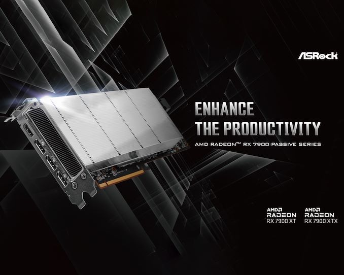
Instead, these groups have been turning to buying up consumer graphics cards, which although they come with additional limitations, are also a fraction of the cost of a "proper" server card. And this week, ASRock has removed another one of those limitations for would-be AMD Radeon users, with the introduction of a set of compact, passively-cooled Radeon RX 7900 XTX and RX 7900 XT video cards that are designed to go in servers.
Without any doubts, ASRock's AMD Radeon RX 7900 XTX Passive 24GB and AMD Radeon RX 7900 XT Passive 20GB AIBs are indeed graphics cards with four display outputs and based on the Navi 31 graphics processor (with 6144 and 5376 stream processors, respectively), so they can output graphics and work both with games and professional applications. And with TGPs of 355W and 315W respectively, these cards aren't underclocked in any way compared to traditional desktop cards. However, unlike a typical desktop card, the cooler on these cards is a dual-slot heatsink without any kind of fan attached, which is meant to be used with high-airflow forced-air cooling.
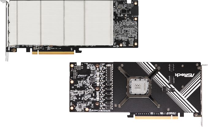
All-told, ASRock's passive cooler is pretty capable, as well; it's not just a simple aluminum heatsink. Beneath the fins, ASRock has gone with a vapor chamber and multiple heat pipes to distribute heat to the rest of the sink. Even with forced-air cooling in racked servers, the heatsink itself still needs to be efficient to keep a 300W+ card cool with only a dual-slot cooler – and especially so when upwards of four of these cards are installed side-by-side with each other. To make the boards even more server friendly, these cards are equipped with a 12V-2×6 power connector, a first for the Radeon RX 7900 series, simplifying installation by reducing cable clutter.
Driving the demand for these cards in particular is their memory configuration. With 24GB for the 7900 XTX and 20GB for the 7900 XT is half as much (or less) memory than can be found on AMD and NVIDIA's high-end professional and server cards, AMD is the only vendor offering consumer cards with this much memory for less than $1000. So for a memory-intensive AI inference cluster built on a low budget, the cheapest 24GB card available starts looking like a tantalizing option.
Otherwise, ASRock's Radeon RX 7900 Passive cards distinguish themselves from AMD's formal professional and server cards by what they're not capable of doing: namely, remote professional graphics or other applications that need things like GPU partitioning. These parts look to be aimed at one application only, artificial intelligence, and are meant to process huge amounts of data. For this purpose, their passive coolers will do the job and the lack of ProViz or VDI-oriented drives ensure that AMD will leave these lucrative markets for itself.
SK hynix to Enter 60 TB SSD Club Next Quarter
Published: Jul 25nd 2024 5:00am on AnandTech
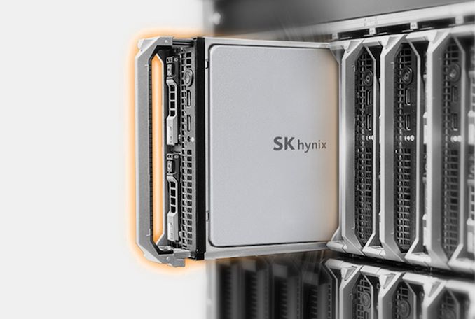
SK hynix this week reported its financial results for the second quarter, as well as offering a glimpse at its plans for the coming quarters. Notably among the company's plans for the year is the release of a SK hynix-branded 60 TB SSD, which will mark the firm's entry into the ultra-premium enterprise SSD league.
"SK hynix plans to expand sales of high-capacity eSSD and lead the market in the second half with 60TB products, expecting eSSD sales to be more than quadrupled compared to last year," a statement by SK hynix reads.
Currently there are only two standard form-factor 61.44 TB SSDs on the market: the Solidigm D5-P5336 (U.2/15mm and E1.L), and the Samsung BM1743 (U.2/15mm and E3.S). Both are built from a proprietary controller (Solidigm's controller still carries an Intel logotype) with a PCIe 4.0 x4 interface and use QLC NAND for storage.
SK hynix's brief mention of the drive means that tere aren't any formal specifications or capabilities to discuss just yet. But it is reasonable to assume that the company will use its own QLC memory for their ultra-high-capacity drives. What's more intriguing are which controller the company plans to use and how it is going to position its 60 TB-class SSD.
Internally, SK hynix has access to multiple controller teams, both of which have the expertise to develop an enterprise-grade controller suitable for a 60 TB drive. SK hynix technically owns Solidigm, the former Intel SSD and NAND unit, giving SK hynix the option of using Solidigm's controller, or even reselling a rebadged D5-P5336 outright. Alternatively, SK hynix has their own (original) internal SSD team, who is responsible for building their well-received Aries SSD controller, among other works.
Ultra-high-capacity SSDs for performance demanding read-intensive storage applications, such as AI inference on the edge or content delivery networks, is a promising premium market. So SK hynix is finding itself highly incentivized to enter it with a compelling offering.
AMD Delays Ryzen 9000 Launch 1 to 2 Weeks Due to Chip Quality Issues
Published: Jul 24nd 2024 6:00am on AnandTech
AMD sends word this afternoon that the company is delaying the launch of their Ryzen 9000 series desktop processors. The first Zen 5 architecture-based desktop chips were slated to launch next week, on July 31st. But citing quality issues that are significant enough that AMD is even pulling back stock already sent to distributors, AMD is delaying the launch by one to two weeks. The Ryzen 9000 launch will now be a staggered launch, with the Ryzen 5 9600X and Ryzen 7 9700X launching on August 8th, while the Ryzen 9 9900X and flagship Ryzen 9 9950X will launch a week after that, on August 15th.
The exceptional announcement, officially coming from AMD’s SVP and GM of Computing and Graphics, Jack Huynh, is short and to the point. Ahead of the launch, AMD found that “the initial production units that were shipped to our channel partners did not meet our full quality expectations.” And, as a result, the company has needed to delay the launch in order to rectify the issue.
Meanwhile, because AMD had already distributed chips to their channel partners – distributors who then filter down to retailers and system builders – this is technically a recall as well, as AMD needs to pull back the first batch of chips and replace them with known good units. That AMD has to essentially take a do-over on initial chip distribution is ultimately what’s driving this delay; it takes the better part of a month to properly seed retailers for a desktop CPU launch with even modest chip volumes, so AMD has to push the launch out to give their supply chain time to catch up.
For the moment, there are no further details on what the quality issue with the first batch of chips is, how many are affected, or what any kind of fix may entail. Whatever the issue is, AMD is simply taking back all stock and replacing it with what they’re calling “fresh units.”
AMD Ryzen 9000 Series Processors Zen 5 Microarchitecture (Granite Ridge) AnandTech Cores / Threads Base Freq Turbo Freq L2 Cache L3 Cache Memory Support TDP Launch Date Ryzen 9 9950X 16C / 32T 4.3GHz 5.7GHz 16 MB 64 MB DDR5-5600 170W 08/15 Ryzen 9 9900X 12C / 24T 4.4GHz 5.6GHz 12 MB 64 MB 120W Ryzen 7 9700X 8C / 16T 3.8GHz 5.5GHz 8 MB 32 MB 65W 08/08 Ryzen 5 9600X 6C / 12T 3.9GHz 5.4GHz 6 MB 32 MB 65WImportantly, however, this announcement is only for the Ryzen 9000 desktop processors, and not the Ryzen AI 300 mobile processors (Strix Point), which are still slated to launch next week. A mobile chip recall would be a much bigger issue (they’re in finished devices that would need significant labor to rework), but also, both the new desktop and mobile Ryzen processors are being made on the same TSMC N4 process node, and have significant overlap in their CPU structures. To be sure, mobile and desktop are very different dies, but it does strongly imply that whatever the issue is, it’s not a design flaw or a fabrication flaw in the silicon itself.
That AMD is able to re-stage the launch of the desktop Ryzen 9000 chips so quickly – on the order of a few weeks – further points to an issue much farther down the line. If indeed the issue isn’t at the silicon level, then that leaves packaging and testing as the next most likely culprit. Whether that means AMD’s packaging partners had some kind of issue assembling the multi-die chips, or if AMD found some other issue that warrants further checks remains to be seen. But it will definitely be interesting to eventually find out the backstory here. In particular I’m curious if AMD is being forced to throw out the first batch of Ryzen 9000 desktop chips entirely, or if they just need to send them through an additional round of QA to pull bad chips.
It’s also interesting here that AMD’s new launch schedule has essentially split the Ryzen 9000 stack in two. The company’s higher-end chips, which incorporate two CCDs, are delayed an additional week over the lower-end units with their single CCD. By their very nature, multi-CCD chips require more time to validate (there’s a whole additional die to test), but they also require more CCDs to assemble. So it’s a toss-up right now whether the additional week for the high-end chips is due to a supply bottleneck, or a chip testing bottleneck.
The silver lining to all of this, at least, is that AMD found the issue before any of the faulty chips made their ways into the hands of consumers. Though the need to re-stage the launch still throws a rather large wrench into marketing efforts of AMD and their partners, a post-launch recall would have been far more disastrous on multiple levels, not to mention that it would have given the company a significant black eye. Something that arch-rival Intel is getting to experience for themselves this week.
In any case, this will certainly go down as one of the more interesting AMD desktop chip launches – and the chips haven’t actually made it out the door yet. We’ll have more on the subject as further details are released. And look forward to chip reviews soon – just not on July 31st as originally planned.
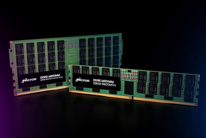
We appreciate the excitement around Ryzen 9000 series processors. During final checks, we found the initial production units that were shipped to our channel partners did not meet our full quality expectations. Out of an abundance of caution and to maintain the highest quality experiences for every Ryzen user, we are working with our channel partners to replace the initial production units with fresh units. As a result, there will be a short delay in retail availability. The Ryzen 7 9700X and Ryzen 5 9600X processors will now go on sale on August 8th, and the Ryzen 9 9950X and Ryzen 9 9900X processors will go on-sale on August 15th. Apologies for the delay. We pride ourselves in providing a high quality experience for every Ryzen user, and we look forward to our fans having a great experience with the new Ryzen 9000 series. -AMD SVP and GM of Computing and Graphics, Jack HuynhMicron Launches 9550 PCIe Gen5 SSDs: 14 GB/s with Massive Endurance
Published: Jul 24nd 2024 1:10am on AnandTech
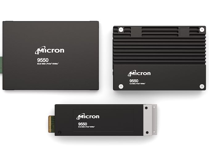
Micron has introduced its Micron 9550-series SSDs, which it claims are the fastest enterprise drives in the industry. The Micron 9550 Pro and 9550 Max SSDs with a PCIe 5.0 x4 interface promise unbeatable performance amid enhanced endurance and power efficiency, which will be particularly beneficial for data centersMicron's 9550-series solid-state drives are based on a proprietary NVMe 2.0b controller with a PCIe Gen5 x4 interface and 232-layer 3D TLC NAND memory. The drives will be available in capacities ranging from 3.2 TB to 30.72 TB with one or three drive writes per day endurance as well as U.2, E1.S, and E3.S form factors to cater to the requirements of different types of servers.
As far as performance is concerned, the Micron 9550 NVMe SSD boasts impressive metrics, including up to sustainable 14.0 GB/s sequential read speeds and 10.0 GB/s sequential write speeds, which is higher compared to the peak performance offered by Samsung's PM1743 SSDs. For random operations, it achieves 3,300 million IOPS in random reads and 0.9 million IOPS in random writes, again surpassing competitor offerings.
Micron says that power efficiency is another standout feature of its Micron 9550 SSD: It consumes up to 81% less SSD energy per terabyte transferred with NVIDIA Magnum IO GPUDirect Storage and up to 35% lower SSD power usage in MLPerf benchmarks compared to rivals. Considering that we are dealing with a claim by the manufacturer itself, the numbers should be taken with caution.
Micron 9550 NVMe Enterprise SSDs 9550 PRO 9550 MAX Form Factor U.2, E1.S, and E3.S U.2, E1.S Interface PCIe 5.0 x4 NVMe 2.0b Capacities 3.84 TB 7.68 TB 15.36 TB 30.72 TB 3.2 TB 6.4 TB 12.8 TB 25.6 TB NAND Micron 232L 3D TLC Sequential Read up to 14,000 MBps Sequential Write up to 10,000 MBps Random Read (4 KB) up to 3.3M IOPS Random Write (4 KB) up to 900K IOPS Power Operating Read: up to 18W Write: up to 16W Idle ? W ? W Write Endurance 1 DWPD 3 DWPD Warranty 5 year""The Micron 9550 SSD represents a giant leap forward for data center storage, delivering a staggering 3.3 million IOPS while consuming up to 43% less power than comparable SSDs in AI workloads such as GNN and LLM training", said Alvaro Toledo, vice president and general manager of Micron's’s Data Center Storage group. "This unparalleled performance, combined with exceptional power efficiency, establishes a new benchmark for AI storage solutions and demonstrates Micron’s unwavering commitment to spearheading the AI revolution."
Micron traditionally offers its high-end data center SSDs in different flavors: the Micron 9550 Pro drives for read-intensive applications are set to be available in 3.84 TB, 7.68 TB, 15.36 TB, and 30.72 TB capacities with one drive writes per day (DWPD) endurance rating, whereas the Micron 9550 Max for mixed-use are set to be available in 3.2 TB, 6.4 TB, 12.8 TB, and 25.6 TB capacities with three DWPD endurance rating. All drives comply with the OCP 2.0 r21 standards and OCP 2.5 telemetry. They also feature SPDM 1.2 and FIPS 140-3 security, secure execution environment, and self-encrypting drive options.
Micron has not touched upon the pricing of the new drives as it depends on volumes and other factors.
JEDEC Plans LPDDR6-Based CAMM, DDR5 MRDIMM Specifications
Published: Jul 23nd 2024 7:00am on AnandTech
Following a relative lull in the desktop memory industry in the previous decade, the past few years have seen a flurry of new memory standards and form factors enter development. Joining the traditional DIMM/SO-DIMM form factors, we've seen the introduction of space-efficient DDR5 CAMM2s, their LPDDR5-based counterpart the LPCAMM2, and the high-clockspeed optimized CUDIMM. But JEDEC, the industry organization behind these efforts, is not done there. In a press release sent out at the start of the week, the group announced that it is working on standards for DDR5 Multiplexed Rank DIMMs (MRDIMM) for servers, as well as an updated LPCAMM standard to go with next-generation LPDDR6 memory.
Just last week Micron introduced the industry's first DDR5 MRDIMMs, which are timed to launch alongside Intel's Xeon 6 server platforms. But while Intel and its partners are moving full steam ahead on MRDIMMs, the MRDIMM specification has not been fully ratified by JEDEC itself. All told, it's not unusual to see Intel pushing the envelope here on new memory technologies (the company is big enough to bootstrap its own ecosystem). But as MRDIMMs are ultimately meant to be more than just a tool for Intel, a proper industry standard is still needed – even if that takes a bit longer.
Under the hood, MRDIMMs continue to use DDR5 components, form-factor, pinout, SPD, power management ICs (PMICs), and thermal sensors. The major change with the technology is the introduction of multiplexing, which combines multiple data signals over a single channel. The MRDIMM standard also adds RCD/DB logic in a bid to boost performance, increase capacity of memory modules up to 256 GB (for now), shrink latencies, and reduce power consumption of high-end memory subsystems. And, perhaps key to MRDIMM adoption, the standard is being implemented as a backwards-compatible extension to traditional DDR5 RDIMMs, meaning that MRDIMM-capable servers can use either RDIMMs or MRDIMMs, depending on how the operator opts to configure the system.
The MRDIMM standard aims to double the peak bandwidth to 12.8 Gbps, increasing pin speed and supporting more than two ranks. Additionally, a "Tall MRDIMM" form factor is in the works (and pictured above), which is designed to allow for higher capacity DIMMs by providing more area for laying down memory chips. Currently, ultra high capacity DIMMs require using expensive, multi-layer DRAM packages that use through-silicon vias (3DS packaging) to attach the individual DRAM dies; a Tall MRDIMM, on the other hand, can just use a larger number of commodity DRAM chips. Overall, the Tall MRDIMM form factor enables twice the number of DRAM single-die packages on the DIMM.
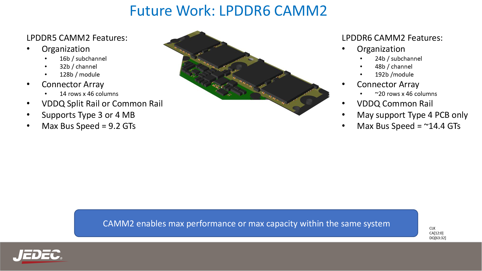
Meanwhile, this week's announcement from JEDEC offers the first significant insight into what to expect from LPDDR6 CAMMs. And despite LPDDR5 CAMMs having barely made it out the door, some significant shifts with LPDDR6 itself means that JEDEC will need to make some major changes to the CAMM standard to accommodate the newer memory type.
 JEDEC Presentation: The CAMM2 Journey and Future Potential
Besides the higher memory clockspeeds allowed by LPDDR6 – JEDEC is targeting data transfer rates of 14.4 GT/s and higher – the new memory form-factor will also incorporate an altogether new connector array. This is to accommodate LPDDR6's wider memory bus, which sees the channel width of an individual memory chip grow from 16-bits wide to 24-bits wide. As a result, the current LPCAMM design, which is intended to match the PC standard of a cumulative 128-bit (16x8) design needs to be reconfigured to match LPDDR6's alterations.
Ultimately, JEDEC is targeting a 24-bit subhannel/48-bit channel design, which will result in a 192-bit wide LPCAMM. While the LPCAMM connector itself is set to grow from 14 rows of pins to possibly as high as 20. New memory technologies typically require new DIMMs to begin with, so it's important to clarify that this is not unexpected, but at the end of the day it means that the LPCAMM will be undergoing a bigger generational change than what we usually see.
JEDEC is not saying at this time when they expect either memory module standard to be completed. But with MRDIMMs already shipping for Intel systems – and similar AMD server parts due a bit later this year – the formal version of that standard should be right around the corner. Meanwhile, LPDDR6 CAMMs will be a bit farther out, particularly as the memory standard itself is still under development.
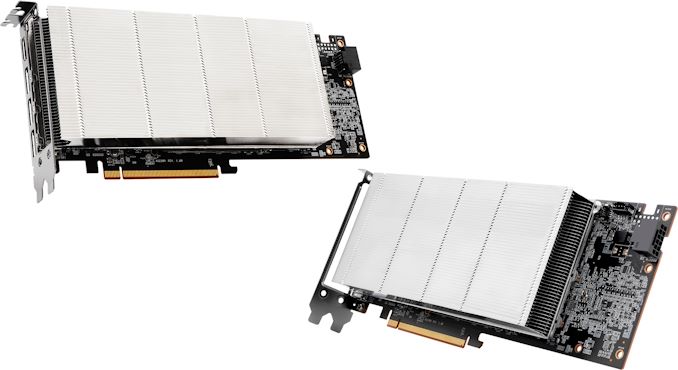
HighPoint Updates NVMe RAID Cards for PCIe 5.0: 50 GBps+ Direct-Attached SSD Storage
Published: Jul 23nd 2024 8:00am on AnandTech
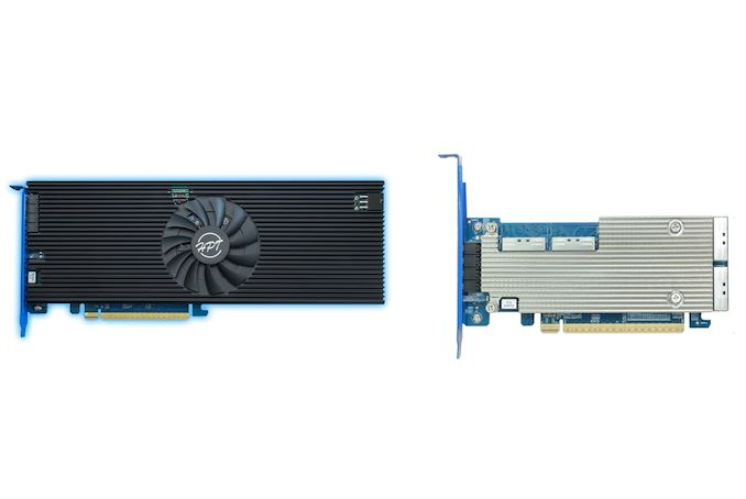
HighPoint Technologies has updated their NVMe switch and RAID solutions with PCIe 5.0, and supporting up to eight NVMe drives. The new HighPoint Rocket 1600 (switch add-in card) and 7600 series (RAID adapters) are the successors to the SSD SSD7500 series adapter cards introduced in 2020. Similar to its predecessors, the new Rocket series cards are also based on a Broadcom PCIe switch (PEX 89048). The Rocket 7600 series runs the RAID stack on the integrated ARM processor (dual-core Cortex A15)
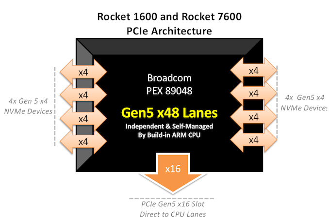
The PEX 89048 supports up to 48 PCIe 5.0 lanes, out of which 16 are dedicated to the host connection in the Rocket adapters. The use of a true PCIe switch means that the product doesn't rely on PCIe lane bifurcation support in the host platform.
HighPoint's Gen 5 stack currently has two products each in the switch and RAID lineups - an add-in card with support for M.2 drives, and a RAID adapter with four 5.0 x8 SFF-TA-1016 (Mini Cool Edge IO or MCIO) connectors for use with backplanes / setups involving U.2 / U.3 / EDSFF drives.
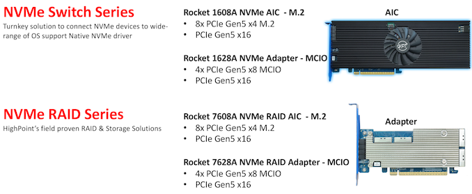
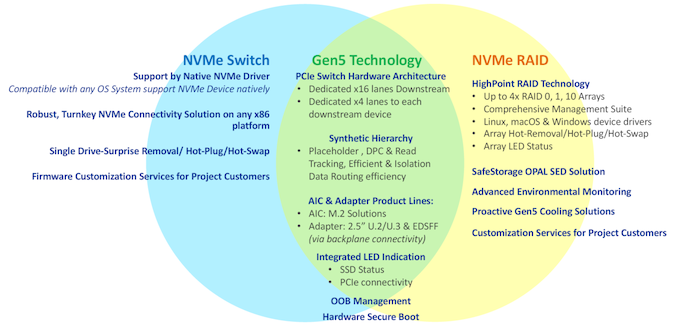
The RAID adapters require HighPoint's drivers (available for Linux, macOS, and Windows), and supports RAID 0, RAID 1, and RAID 10 arrays. On the other hand, the AIC requires no custom drivers. RAID configurations with the AIC will need to be handled by software running on the host OS. On the hardware side, all members of the Rocket series come with an external power connector (as the solution can consume upwards of 75W) and integrate a heatsink. The M.2 version is actively cooled, as the drives are housed within the full-height / full-length cards.
The solution can theoretically support up to 64 GBps of throughput, but real-world performance is limited to around 56 GBps using Gen 5 drives. It must be noted that even Gen 4 drives can take advantage of the new platform and deliver better performance with the new Rocket series compared to the older SSD7500 series.
The cards are shipping now, with pricing ranging from $1500 (add-in card) to $2000 (RAID adapters). HighPoint is not alone in targeting this HEDT / workstation market. Sabrent has been teasing their Apex Gen 5.0 x16 solution involving eight M.2 SSDs for a few months now (involving a Microchip PCIe switch. Until that solution comes to the market, HighPoint appears to be the only game in town for workstation users requiring access to direct-attached storage capable of delivering 50 GBps+ speeds.
Intel Addresses Desktop Raptor Lake Instability Issues: Faults Excessive Voltage from Microcode, Fix Coming in August
Published: Jul 22nd 2024 7:00am on AnandTech
In what started last year as a handful of reports about instability with Intel's Raptor Lake desktop chips has, over the last several months, grown into a much larger saga. Facing their biggest client chip instability impediment in decades, Intel has been under increasing pressure to figure out the root cause of the issue and fix it, as claims of damaged chips have stacked up and rumors have swirled amidst the silence from Intel. But, at long last, it looks like Intel's latest saga is about to reach its end, as today the company has announced that they've found the cause of the issue, and will be rolling out a microcode fix next month to resolve it.
Officially, Intel has been working to identify the cause of desktop Raptor Lake’s instability issues since at least February of this year, if not sooner. In the interim they have discovered a couple of correlating factors – telling motherboard vendors to stop using ridiculous power settings for their out-of-the-box configurations, and finding a voltage-related bug in Enhanced Thermal Velocity Boost (eTVB) – but neither factor was the smoking gun that set all of this into motion. All of which had left Intel to continue searching for the root cause in private, and lots of awkward silence to fill the gaps in the public.
But it looks like Intel’s search has finally come to an end – even if Intel isn’t putting the smoking gun on public display quite yet. According to a fresh update posted to the company’s community website, Intel has determined the root cause at last, and has a fix in the works.
Per the company’s announcement, Intel has tracked down the cause of the instability issue to “elevated operating voltages”, that at its heart, stems from a flawed algorithm in Intel’s microcode that requested the wrong voltage. Consequently, Intel will be able to resolve the issue through a new microcode update, which pending validation, is expected to be released in the middle of August.
Based on extensive analysis of Intel Core 13th/14th Gen desktop processors returned to us due to instability issues, we have determined that elevated operating voltage is causing instability issues in some 13th/14th Gen desktop processors. Our analysis of returned processors confirms that the elevated operating voltage is stemming from a microcode algorithm resulting in incorrect voltage requests to the processor. Intel is delivering a microcode patch which addresses the root cause of exposure to elevated voltages. We are continuing validation to ensure that scenarios of instability reported to Intel regarding its Core 13th/14th Gen desktop processors are addressed. Intel is currently targeting mid-August for patch release to partners following full validation. Intel is committed to making this right with our customers, and we continue asking any customers currently experiencing instability issues on their Intel Core 13th/14th Gen desktop processors reach out to Intel Customer Support for further assistance. -Intel Community PostAnd while there’s nothing good for Intel about Raptor Lake’s instability issues or the need to fix them, that the problem can be ascribed to (or at least fixed by) microcode is about the best possible outcome the company could hope for. Across the full spectrum of potential causes, microcode is the easiest to fix at scale – microcode updates are already distributed through OS updates, and all chips of a given stepping (millions in all) run the same microcode. Even a motherboard BIOS-related issue would be much harder to fix given the vast number of different boards out there, never mind a true hardware flaw that would require Intel to replace even more chips than they already have.
Still, we’d also be remiss if we didn’t note that microcode is regularly used to paper over issues further down in the processor, as we’ve most famously seen with the Meltdown/Spectre fixes several years ago. So while Intel is publicly attributing the issue to microcode bugs, there are several more layers to the onion that is modern CPUs that could be playing a part. In that respect, a microcode fix grants the least amount of insight into the bug and the performance implications about its fix, since microcode can be used to mitigate so many different issues.
But for now, Intel’s focus is on communicating that they have fix and establishing a timeline for distributing it. The matter has certainly caused them a lot of consternation over the last year, and it will continue to do so for at least another month.
In the meantime, we’ve reached out to our Intel contacts to see if the company will be publishing additional details about the voltage bug and its fix. “Elevated operating voltages” is not a very satisfying answer on its own, and given the unprecedented nature of the issue, we’re hoping that Intel will be able to share additional details as to what’s going on, and how Intel will be preventing it in the future.
Intel Also Confirms a Via Oxidation Manufacturing Issue Affected Early Raptor Lake ChipsTangential to this news, Intel has also made a couple of other statements regarding chip instability to the press and public over the last 48 hours that also warrant some attention.
First and foremost, leading up to Intel’s official root cause analysis of the desktop Raptor Lake instability issues, one possibility that couldn’t be written off at the time was that the root cause of the issue was a hardware flaw of some kind. And while the answer to that turned out to be “no,” there is a rather important “but” in there, as well.
As it turns out, Intel did have an early manufacturing flaw in the enhanced version of the Intel 7 process node used to build Raptor Lake. According to a post made by Intel to Reddit this afternoon, a “via Oxidation manufacturing issue” was addressed in 2023. However, despite the suspicious timing, according to Intel this is separate from the microcode issue driving instability issues with Raptor Lake desktop processors up to today.
Short answer: We can confirm there was a via Oxidation manufacturing issue (addressed back in 2023) but it is not related to the instability issue. Long answer: We can confirm that the via Oxidation manufacturing issue affected some early Intel Core 13th Gen desktop processors. However, the issue was root caused and addressed with manufacturing improvements and screens in 2023. We have also looked at it from the instability reports on Intel Core 13th Gen desktop processors and the analysis to-date has determined that only a small number of instability reports can be connected to the manufacturing issue. For the Instability issue, we are delivering a microcode patch which addresses exposure to elevated voltages which is a key element of the Instability issue. We are currently validating the microcode patch to ensure the instability issues for 13th/14th Gen are addressed. -Intel Reddit PostUltimately, Intel says that they caught the issue early-on, and that only a small number of Raptor Lake were affected by the via oxidation manufacturing flaw. Which is hardly going to come as a comfort to Raptor Lake owners who are already worried about the instability issue, but if nothing else, it’s helpful that the issue is being publicly documented. Typically, these sorts of early teething issues go unmentioned, as even in the best of scenarios, some chips inevitably fail prematurely.
Unfortunately, Intel’s revelation here doesn’t offer any further details on what the issue is, or how it manifests itself beyond further instability. Though at the end of the day, as with the microcode voltage issue, the fix for any affected chips will be to RMA them with Intel to get a replacement.
Laptops Not Affected by Raptor Lake Microcode IssueFinally, ahead of the previous two statements, Intel also released a statement to Digital Trends and a few other tech websites over the weekend, in response to accusations that Intel’s 13th generation Core mobile CPUs were also impacted by what we now know to be the microcode flaw. In the statement, Intel refuted those claims, stating that laptop chips were not suffering from the same instability issue.
Intel is aware of a small number of instability reports on Intel Core 13th/14th Gen mobile processors. Based on our in-depth analysis of the reported Intel Core 13th/14th Gen desktop processor instability issues, Intel has determined that mobile products are not exposed to the same issue. The symptoms being reported on 13th/14th Gen mobile systems – including system hangs and crashes – are common symptoms stemming from a broad range of potential software and hardware issues. As always, if users are experiencing issues with their Intel-powered laptops we encourage them to reach out to the system manufacturer for further assistance. -Intel Rep to Digital TrendsInstead, Intel attributed any laptop instability issues to typical hardware and software issues – essentially claiming that they weren’t experiencing elevated instability issues. Whether this statement accounts for the via oxidation manufacturing issue is unclear (in large part because not all 13th Gen Core Mobile parts are Raptor Lake), but this is consistent with Intel’s statements from earlier this year, which have always explicitly cited the instability issues as desktop issues.
Tenstorrent Launches Wormhole AI Processors: 466 FP8 TFLOPS at 300W
Published: Jul 19nd 2024 2:30am on AnandTech
Tenstorrent has unveiled its next-generation Wormhole processor for AI workloads that promises to offer decent performance at a low price. The company currently offers two add-on PCIe cards carrying one or two Wormhole processors as well as TT-LoudBox, and TT-QuietBox workstations aimed at software developers. The whole of today's release is aimed at developers rather than those who will deploy the Wormhole boards for their commercial workloads.
“It is always rewarding to get more of our products into developer hands. Releasing development systems with our Wormhole™ card helps developers scale up and work on multi-chip AI software.” said Jim Keller, CEO of Tenstorrent. “In addition to this launch, we are excited that the tape-out and power-on for our second generation, Blackhole, is going very well.”
Each Wormhole processor packs 72 Tensix cores (featuring five RISC-V cores supporting various data formats) with 108 MB of SRAM to deliver 262 FP8 TFLOPS at 1 GHz at 160W thermal design power. A single-chip Wormhole n150 card carries 12 GB of GDDR6 memory featuring a 288 GB/s bandwidth.
Wormhole processors offer flexible scalability to meet the varying needs of workloads. In a standard workstation setup with four Wormhole n300 cards, the processors can merge to function as a single unit, appearing as a unified, extensive network of Tensix cores to the software. This configuration allows the accelerators to either work on the same workload, be divided among four developers or run up to eight distinct AI models simultaneously. A crucial feature of this scalability is that it operates natively without the need for virtualization. In data center environments, Wormhole processors will scale both inside one machine using PCIe or outside of a single machine using Ethernet.
From performance standpoint, Tenstorrent's single-chip Wormhole n150 card (72 Tensix cores at 1 GHz, 108 MB SRAM, 12 GB GDDR6 at 288 GB/s) is capable of 262 FP8 TFLOPS at 160W, whereas the dual-chip Wormhole n300 board (128 Tensix cores at 1 GHz, 192 MB SRAM, aggregated 24 GB GDDR6 at 576 GB/s) can offer up to 466 FP8 TFLOPS at 300W (according to Tom's Hardware).
To put that 466 FP8 TFLOPS at 300W number into context, let's compare it to what AI market leader Nvidia has to offer at this thermal design power. Nvidia's A100 does not support FP8, but it does support INT8 and its peak performance is 624 TOPS (1,248 TOPS with sparsity). By contrast, Nvidia's H100 supports FP8 and its peak performance is massive 1,670 TFLOPS (3,341 TFLOPS with sparsity) at 300W, which is a big difference from Tenstorrent's Wormhole n300.
There is a big catch though. Tenstorrent's Wormhole n150 is offered for $999, whereas n300 is available for $1,399. By contrast, one Nvidia H100 card can retail for $30,000, depending on quantities. Of course, we do not know whether four or eight Wormhole processors can indeed deliver the performance of a single H300, though they will do so at 600W or 1200W TDP, respectively.
In addition to cards, Tenstorrent offers developers pre-built workstations with four n300 cards inside the less expensive Xeon-based TT-LoudBox with active cooling and a premium EPYC-powered TT-QuietBox with liquid cooling.
Sources: Tenstorrent, Tom's Hardware
Gallery: Tenstorrent Launches Wormhole AI Processors: 466 FP8 TFLOPS at 300W
