Solidigm D7-PS1010 and D7-PS1030: PCIe 5.0 and 176L TLC Datacenter SSD Performance Play
Published: Aug 6nd 2024 11:00am on AnandTech
Solidigm's datacenter SSD lineup includes models targeting different performance, endurance, and cost tradeoffs. Last year, the company had introduced the D5-P5336 QLC drive as a low-cost high-capacity drive for read-heavy workloads, while also preparing the SLC-based D7-P5810 for extremely write-intensive workloads requiring high endurance. The D7-P5520 / D7-P5620 Gen 4 drives with Solidigm's own 144L 3D TLC have been the high-performance offerings for generic workloads over the last couple of years.
Solidigm is announcing the availability of the successor to the D7-P5x20 today - the new D7-PS1010 and D7-PS1030. Both of these NVMe drives use SK hynix's 176L 3D TLC NAND and come with a PCIe 5.0 interface. The third digit in the model number matches the DWPD rating, with the D7-PS1010 targeting mixed workloads with a 1 DWPD rating, and the D7-PS1030 targeting write-intensive use-cases with a 3 DWPD rating.
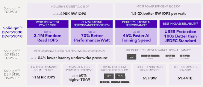
Compared to the previous generation D7-P5x20, the D7-PS10x0 series brings about the following upgrades:
- Move from PCIe 4.0 x4 to PCIe 5.0 x4
- Move from 144L floating gate 3D TLC (Solidigm) to 176L charge trap 3D TLC (SK hynix)
- 25% longer mean-time between failures (MTBF) at 2.5M hours
- 10x higher uncorrectable bit-error rate (UBER) at 1E-18
- 1.8x to 2.8x improvement in high queue-depth random access IOPS
- 2.0x to 2.2x improvement in high queue-depth sequential access throughput
The specifications of the two new SSD families are summarized in the table below.
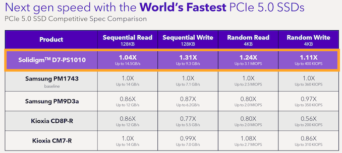
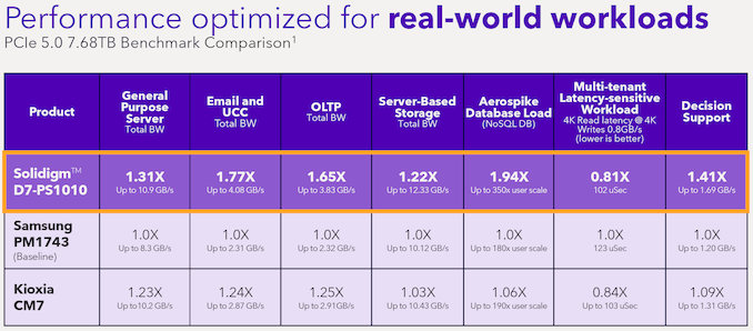
Solidigm D7-PS1000 Series Enterprise SSDs D7-PS1030 D7-P1010 Form Factor U.2 2.5" 15mm E3.S 7.5mm Interface PCIe 5.0 NVMe 2.0 Capacities 1.6TB 3.2TB 6.4TB 12.8TB 1.92TB 3.68TB 7.68TB 15.36TB NAND SK hynix 176L 3D TLC (Charge Trap Architecture) Sequential Read (128 KB @ QD 128) 14500 MB/s Sequential Write (128 KB @ QD 128) 4100 MB/s (1.6 TB / 1.92 TB) 8200 MB/s (3.2 TB / 3.84 TB) 9300 MB/s (6.4 TB / 7.68 TB / 12.8 TB / 15.36 TB) Random Read (4 KB @ QD 512) 2.35 M (1.6 TB / 1.92 TB) 3.1 M (3.2 TB / 3.84 TB) 2.8 M (6.4 TB / 7.68 TB) 2.75 M (12.8 TB / 15.36 TB) Random Write (4 kB) 0.35 M (1.6 TB) 0.716 M (3.2 TB) 0.8 M (6.4 TB / 12.8 TB) 0.15 M (1.92 TB) 0.315 M (3.84 TB) 0.4 M (7.68 TB) 0.38 M (15.36 TB) Power Sustained Write 13 W (1.6 TB / 1.92 TB) 18 W (3.2 TB / 3.84 TB) 23 W (6.4 TB / 7.68 TB / 12.8 TB / 15.36 TB) Sustained Read 17 W (1.6 TB / 1.92 TB) 19 W (3.2 TB / 3.84 TB) 22 W (6.4 TB / 7.68 TB) 23 W (12.8 TB / 15.36 TB) Peak 18 W (1.6 TB / 1.92 TB) 22 W (3.2 TB / 3.84 TB) 29 W (6.4 TB / 7.68 TB) 30 W (12.8 TB / 15.36 TB) Idle 5 W Write Endurance 3 DWPD 1 DWPD Warranty 5 yearsBased on Solidigm's own internal testing, the D7-PS1010 compares very favorably against the Gen 5 datacenter SSDs already in the market from Samsung and Kioxia. However, the recently introduced Micron 9550 series may present a better challenge to Solidigm's claims.
Gen 5 SSDs are well-suited for the storage-intensive tasks in AI workloads. Every new product needs to tie itself to the AI buzzword currently, but we should excuse SSD manufacturers for doing the same - after all training and inference needs to move large amounts of data back and forth between the processing engine and underlying memory. Solidigm expects the D7-PS10x0 to be a good fit as direct-attached storage internal to GPU servers or as all-flash tier supporting a HDD-only object tier in the cloud. For on-premises GPU servers, the flash / HDD tiered storage can be replaced by an all-QLC object tier.
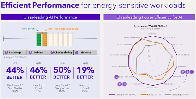
Solidigm claims better energy efficiency compared to the competitors' Gen 5 drives from last year for various AI workload traces. While the data ingest and archival processes require system designers to maximize the storage capacity per watt (the QLC-based Solidigm D5-P5336 is attractive here), the core processing steps require the optimization of performance per watt. The D7-PS10x0 have a natural fit in this segment.
Solidigm / Intel has been serving the datacenter SSD market since its inception. The company is well aware of the quality and reliability requirements in this space. The D7-PS1010 and D7-PS1030 include the usual enhanced PLI (power loss imminent) validation checks for data saved in the process of power loss / restoration. The critical SRAMs in the SSD controller also have ECC protection. UBER testing goes well beyond the suggested JEDEC specifications. The company also claims that its silent data corruption testing and modeling are better than its competitors.
The new D7-PS1010 and D7-PS1030 bring class-leading Gen 5 performance to the datacenter SSD market. They are available for purchase now in both U.2 and E3.S form factors, with capacities ranging from 1.6 TB - 12.8 TB (D7-PS1030) and 1.92 TB - 15.36 TB (D7-PS1010).
Samsung Shrinks LPDDR5X Chips by 9%, Now Just 0.65mm Thick
Published: Aug 5nd 2024 7:00am on AnandTech
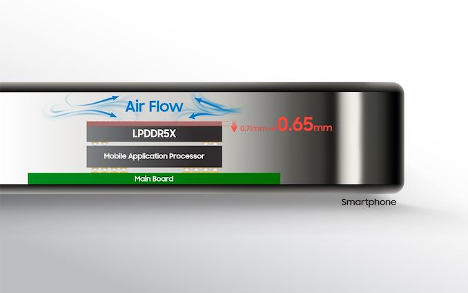
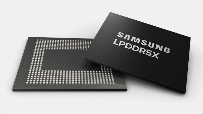
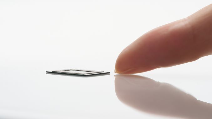
Samsung is announcing today that it has begun mass production of 12 GB and 16 GB LPDDR5X modules in the industry's thinnest package. Samsung's shrunken memory packages measure approximately 0.65 mm in thickness, making them 0.06 mm (~9%) thinner than standard LPDDR5X packages. The company expects the new DRAM devices to be used to make for thinner smartphones, or improve their performance by enabling better airflow inside.
According to the company's press release, Samsung achieved this ultra-thin design by employing new packaging methods, such as optimized printed circuit boards (PCBs) and epoxy molding compound (EMC). Additionally, an optimized back-lapping process was used to further reduce the height of the packages. The newly developed DRAM packages are not only thinner by 9% compared to previous models but also offer a 21.2% improvement in heat resistance.
Thinner LPDDR5X packaging help enhance airflow within smartphones, significantly improving thermal management, which means higher performance and longer battery life. Also, better thermal management help to prolong device's lifespan.
"Samsung's LPDDR5X DRAM sets a new standard for high-performance on-device AI solutions, offering not only superior LPDDR performance but also advanced thermal management in an ultra-compact package," said YongCheol Bae, Executive Vice President of Memory Product Planning at Samsung Electronics. "We are committed to continuous innovation through close collaboration with our customers, delivering solutions that meet the future needs of the low-power DRAM market."
While Samsung's thinner LPDDR5X DRAM packages contribute to making smartphones slimmer, they are just one part of the overall design strategy. Other components, such as thinner protective glass, PCBs, and batteries, play considerably more significant roles in reducing device thickness. Meanwhile, the primary benefit of these new memory modules may be in improving airflow inside smartphones.
Samsung is looking to further expand its LPDDR5X product lineups by developing even more compact packages, including 6-layer 24 GB and 8-layer 32 GB modules. Specific details about the thickness of these future memory modules have not yet been disclosed, though making high-capacity DRAMs thinner in general is an important thing.
Western Digital: We Are Sampling 32TB SMR Hard Drives
Published: Aug 2nd 2024 10:00am on AnandTech

In an unexpected announcement during their quarterly earnings call this week, Western Digital revealed that it has begun sampling an upcoming 32TB hard drive. The nearline HDD is aimed at hyperscalers, and relies on a combination of Westen Digital's EAMR technology, as well as shingled magnetic recording (SMR) technology to hit their highest capacity figures to date.
Western Digital's 32TB HDD uses all of the company's most advanced technologies. Besides energy-assisted magnetic recording (EAMR/ePMR 2 to be more precise) technology, WD is also leveraging triple-stage actuators for better positioning of heads and two-dimensional (TDMR) read heads, OptiNAND for extra performance and reliability, distributed sector (DSEC) technology and a proprietary error correcting code (ECC) technology. And, most importantly, UltraSMR technology to provide additional capacity.
"We are shipping samples of our 32TB UltraSMR/ePMR nearline hard drives to select customers," said David Goeckeler, chief executive of Western Digital, at the earnings call. "These drives feature advanced triple-stage actuators and OptiNAND technology which are designed for seamless qualification, integration and deployment in hyperscale cloud and enterprise data centers while maintaining exceptional reliability."
Seagate is currently shipping its 30TB Exos HDDs based on heat-assisted magnetic recording (HAMR) platform called Modaic 3+ to select exascalers, and the company has implied that it can build a 32TB version of the drive using SMR. Therefore, from capacity point of view, Western Digital's announcement means that the company has caught up with its rival.
As with the comapny's other UltraSMR drives, the 32TB nearline drive is aimed at WD's enterprise customers, whose infrastructure can handle the additional management requirements that SMR imposes. As SMR in enterprise drives is not transparent, it's up to the host to manage many of the complexities that come with a hard drive that isn't suited for random writes. Though at least in WD's case, the upshot is that UltraSMR also offers a more significant density increase than other SMR implementations, using a larger number of SMR bands to increase HDD capacity by up to 20%.
Working backwards, that 20% capacity increase also means that WD's new drive is starting from 2.56TB CMR platters. And while 2.56TB makes for a very decent areal density, this would mean that WD is still behind rival Seagate in terms of areal density overall, as Seagate has 3TB CMR platters in its latest HAMR-based Exos drives.
ECS LIVA Z5 PLUS mini-PC Review: A Different Take on Raptor Lake
Published: Aug 2nd 2024 8:45am on AnandTech
The trend towards miniaturization of desktop systems was kickstarted by the Intel NUCs in the early 2010s. The increasing popularity of compact PCs also led to the introduction of a variety of slightly larger form-factors. Custom boards falling in size between the NUC's 4" x 4" ultra-compact form-factor (UCFF) and industrial-applications oriented 3.5" SBC have also gained traction. The ECS LIVA Z5 PLUS is one such system, designed and marketed towards business and industrial use-cases.
Intel's Raptor Lake series of products was introduced in early 2023. It came in both P and U versions for notebooks and ultraportables, in addition to the usual H(X) ones for high-performance gaming notebooks. Most mini-PCs and NUCs opted for the P varieties in their systems. The ECS LIVA Z5 PLUS represents a different take, with a U series processor operating with a slight increase in the configurable TDP (cTDP) over Intel's suggested 15W operating point. Read on for a comprehensive look at the performance and features of the ECS LIVA Z5 PLUS, including some comments on the benefits enabled by the slightly larger form-factor.
Intel Extends 13th & 14th Gen Core Retail CPU Warranties By 2 Years In Response to Chip Instability Issues
Published: Aug 2nd 2024 8:00am on AnandTech
Capping off an extensive (and expensive) week for Intel, the company has also announced that they are taking additional steps to address the ongoing chip stability issues with desktop Raptor Lake chips – the 13th and 14th Generation desktop Core processors. In order to keep owners whole, Intel will be extending the warranty on retail boxed Raptor Lake chips by two years, bringing the cumulative warranty for the chips to five years altogether.
This latest announcement comes as Intel is still in the process of preparing their major Raptor Lake microcode update, which is designed to mitigate the issue (or rather, further damage) by fixing the elevated voltage bug in their existing microcode that has led to the issue in the first place. That microcode update remains scheduled for mid-August, roughly a couple of weeks from now.
But until then – and depending on how quickly the update is distributed, even afterwards – there is still the matter of what to do with Raptor Lake desktop chips that are already too far gone and are consequently unstable. Intel’s retail boxed Raptor Lake chips ship with a 3 year warranty, which given the October 2022 launch date, would have the oldest of these chips covered until October of 2025 – a bit over a year from now. And while the in-development fix should mean that this is plenty of time to catch and replace any damaged chips, Intel has opted to take things one step further by extending the chips’ warranty to five years.
Overall, this is much-needed bit of damage control by Intel to restore some faith in their existing Raptor Lake desktop processor lineup. Even with the planned microcode fix, it remains unclear at best about what the long-term repercussions of the voltage bug is, and what it means for the lifespan of still-stable chips that receive the fixed microcode. In the best-case scenario, an extended warranty gives Raptor Lake owners a bit more peace of mind, and in a worst-case scenario, they’re now covered for a couple of years longer if the chip degradation issues persist.
One important thing to note, however, is that the extended warranty will only apply to boxed processors, i.e. Intel’s official retail chips. Intel’s loose chips that are sold by the tray to OEMs and certain distributors – commonly referred to as “tray” processors – are not covered by the extended warranty. While Raptor Lake tray processors do technically come with a three-year warranty of their own, Intel does not provide direct, end-user warranty service for these chips. Instead, those warranties are serviced by the OEM or distributor that sold the chip.
With the bulk of Intel’s chips going to OEMs and other professional system builders, Intel will undoubtedly need to settle things with those groups, as well. But with OEM dealings typically remaining behind closed doors, it’s unlikely we’ll hear about just what is agreed there. Regardless, whatever Intel does (or doesn’t do) to assuage OEMs and distributors, those groups will remain responsible for handling warranty claims for tray chips.
Finally, it should be noted that while today’s announcement outlines the two-year warranty extension, it doesn’t deliver the full details on the program. Intel expects to release more details on the extended warranty program “in the coming days.”
Intel’s full statement is below:
Intel is committed to making sure all customers who have or are currently experiencing instability symptoms on their 13th and/or 14th Gen desktop processors are supported in the exchange process. We stand behind our products, and in the coming days we will be sharing more details on two-year extended warranty support for our boxed Intel Core 13th and 14th Gen desktop processors. In the meantime, if you are currently or previously experienced instability symptoms on your Intel Core 13th/14th Gen desktop system:- For users who purchased systems from OEM/System Integrators – please reach out to your system manufacturer’s support team for further assistance.
- For users who purchased a boxed CPU – please reach out to Intel Customer Support for further assistance.
Separately, Intel’s community team also posted a brief update on the via oxidation issue that, although distinct from the current Raptor Lake instability issues, came into question at roughly the same time. Intel has previously stated that that issue is unconnected to the ongoing stability issues, and was fixed back in 2023. And this latest update offers a few more details on just what that manufacturing issue entailed.
The Via Oxidation issue currently reported in the press is a minor one that was addressed with manufacturing improvements and screens in early 2023. The issue was identified in late 2022, and with the manufacturing improvements and additional screens implemented Intel was able to confirm full removal of impacted processors in our supply chain by early 2024. However, on-shelf inventory may have persisted into early 2024 as a result. Minor manufacturing issues are an inescapable fact with all silicon products. Intel continuously works with customers to troubleshoot and remediate product failure reports and provides public communications on product issues when the customer risk exceeds Intel quality control thresholds. -Intel Community PostReport: Intel Meteor Lake In Short Supply Due to Yield Issues, Intel Running Hot Lots
Published: Aug 1nd 2024 8:15am on AnandTech
Alongside Intel’s weak Q2 2024 earnings report and the announcement of $10 billion in spending cuts for 2025, the company is also relaying one other piece of bad news regarding its current chip deliveries. A brief report, posted on X by analyst Patrick Moorhead and citing a conversation with Intel CEO Pat Gelsinger, revealed that Intel has been dealing with a yield issue on Meteor Lake, with the issue being significant enough to drive intel to take extraordinary steps to deliver the necessary chips.
It was a very rough Q2 for $INTC. And that guide... Thanks, @Pgelsinger, for the time to discuss. It appears that there were yield/throughput issues on Meteor Lake, negatively impacting gross margins. When you have to get the product to your customers, and you have wafers to… pic.twitter.com/pHU66xvFe7
— Patrick Moorhead (@PatrickMoorhead) August 1, 2024 It appears that there were yield/throughput issues on Meteor Lake, negatively impacting gross margins. When you have to get the product to your customers, and you have wafers to burn, you run it hot. I heard from OEMs that they needed more MTL, but it wasn't bone dry. You have to run hot lots in that case, or else your customers will be impacted. I didn't have this one on my dance card. -Patrick MoorheadDecoding Moorhead’s dense tweet, the biggest revelation here is that Intel has been suffering from yield issues on Meteor Lake. The first chip from the company to incorporate Intel’s EUV-augmented Intel 4 process, Meteor Lake was not expected to be particularly high yielding at the start (no lead chip for a new process node ever is). However, without citing specific figures, Moorhead’s report implies that Intel’s yield – and resulting Meteor Lake chip throughput – were worse than even the modest expectations that come with a new node.
Most interesting of all here is the claim that Intel has been running production “hot lots” of Meteor Lake – high priority wafer batches that get moved to the front of the line in order to be processed as soon as possible (or as reasonably close as is practical). Hot lots are typically used to get highly-demanded chips produced quickly, getting them through a fab more quickly than the normal process would take. As a business tool, hot lots are a fact of life of chip production, but they’re undesirable because in most cases they cause disruptions to other wafers that are waiting their turn to be processed.
The situation with Meteor Lake is somewhat particular, as the Intel 4 process used for Meteor Lake’s compute tile (the only active tile made at Intel) is not offered to external foundry customers, or even used by other Intel CPUs (Xeon 6s all use Intel 3). As a result, Intel’s capacity is all their own, hence Moorhead’s comment on having “wafers to burn”. In short, it seems Intel slammed through a large number of wafers – yields be damned – in order to produce more Meteor Lake chips to satisfy OEMs.
And the tactic seems to have worked. Intel reported in their Q2 earnings that they’ve shipped 15 million “AI PC” chips since Meteor Lake’s launch, which is still a significant number of chips. So whatever Meteor Lake’s yields are, they are not so dire that Intel is struggling to get any chips out; only that they weren’t getting enough chips out. In this case, according to Moorhead, OEMs would have taken more chips if they were available.
As for the total costs to Intel for running Meteor Lake hot lots and not being able to deliver enough chips, these are reflected both in regards to Intel’s client chip revenue, and their gross margins. Revenue is fairly straightforward: Intel could have sold more chips if they had them. As for gross margins, the company cited lower gross margins for the quarter due to “headwinds from the accelerated ramp of our AI PC product,” which lower-than-expected chip yields would certainly lead to.
There is also the matter of the wafers that got bumped to make room for those Meteor Lake hot lots. Intel 4 has significant overlap with Intel 3 (the latter is a refined version of Intel 4), but as Intel’s lead products for Intel 3 are their high-margin Xeon products, it seems unlikely that they bumped anything related to those in favor of client chips. More likely any bumps were on tools shared with the Intel 7 node, but it’s unlikely we’ll ever hear the full details there.
In any case, Intel at this point is looking to turn around their troubled fortunes in the second half of this year. The company’s next-gen client SoC for mobile, Lunar Lake, is set to launch on September 3rd. And notably, both of its active tiles are being built by TSMC. So Lunar Lake would be spared from any Intel fab snafus, though it still has to go through Intel’s facilities for assembly using their Foveros technology.
Intel Bleeds Red, Plans 15% Workforce Layoff and $10B Cuts For 2025
Published: Aug 1nd 2024 7:15am on AnandTech
Amidst the backdrop of a weak quarterly earnings report that saw Intel lose money for the second quarter in a row, Intel today has announced that the company will be cutting costs by $10 billion in 2025 in an effort to bring Intel back to profitability. The cuts will touch almost every corner of the company in some fashion, with Intel planning to cut spending on R&D, marketing, administration, and capital expenditures. The most significant of these savings will come from a planned 15% reduction in force, which will see Intel lay off 15,000 employees over the next several months – thought to be one of Intel’s biggest layoffs ever.
In an email to Intel’s staff, which was simultaneously published to Intel’s website, company CEO Pat Gelsinger made the financial stakes clear: Intel is spending an unsustainable amount of money for their current revenues. Citing the company’s current costs, Gelsinger wrote that “our costs are too high, our margins are too low,“ and that “our annual revenue in 2020 was about $24 billion higher than it was last year, yet our current workforce is actually 10% larger now than it was then.” Consequently, Intel will be enacting a series of painful cuts to bring the company back to profitability.
Intel is not publicly disclosing precisely where those cuts will come from, but in the company’s quarterly earnings release, the company noted that it was targeting operating expenses, capital expenditures, and costs of sales alike.
For operating expenses, Intel will be cutting “non-GAAP R&D and marketing, general and administrative” spending, with a goal to trim that from $20 billion in 2024 to $17.5 billion in 2025. Meanwhile gross capital expenditures, a significant expense for Intel in recent years as the company has built up its fab network, are projected to drop from $25 billion to $27 billion for 2024, to somewhere between $20 billion and $23 billion in 2025. Compared to Intel’s previous plans for capital expenditures, this would reduce those costs by around 20%. And finally, the company is expecting to save $1 billion on the cost of sales in 2025.
Intel 2025 Spending Cuts 2024 Projected Spending 2025 Projected Spending Projected Reduction Operating Expenses (R&D, Marketing, General, & Admin) $20B $17.5B $2.5B Capital Expenditures $25B - $27B $20B - $23B $2B - $7B Cost of Sales N/A $1B Savings $1BSeparately, in Intel’s email to its employees, Gelsinger outlined that these cuts will also require simplifying Intel’s product portfolio, as well as the company itself. The six key priorities for Intel will include cutting underperforming product lines, and cutting back Intel’s investment in new products to “fewer, more impactful projects”. Meanwhile on the administrative side of efforts, Intel is looking to eliminate redundancies and overlap there, as well as stopping non-essential work.
- Reducing Operational Costs: We will drive companywide operational and cost efficiencies, including the cost savings and head count reductions mentioned above.
- Simplifying Our Portfolio: We will complete actions this month to simplify our businesses. Each business unit is conducting a portfolio review and identifying underperforming products. We are also integrating key software assets into our business units so we accelerate our shift to systems-based solutions. And we will narrow our incubation focus on fewer, more impactful projects.
- Eliminating Complexity: We will reduce layers, eliminate overlapping areas of responsibility, stop non-essential work, and foster a culture of greater ownership and accountability. For example, we will consolidate Customer Success into the Sales, Marketing and Communications Group to streamline our go-to-market motions.
- Reducing Capital and Other Costs: With the completion of our historic five-nodes-in-four-years roadmap clearly in sight, we will review all active projects and equipment so we begin to shift our focus toward capital efficiency and more normalized spending levels. This will reduce our 2024 capital expenditures by more than 20%, and we plan to reduce our non-variable cost of goods sold by roughly $1 billion in 2025.
- Suspending Our Dividend: We will suspend our stock dividend beginning next quarter to prioritize investments in the business and drive more sustained profitability.
- Maintaining Growth Investments: Our IDM2.0 strategy is unchanged. Having fought hard to reestablish our innovation engine, we will maintain the key investments in our process technology and core product leadership.
The bulk of these cuts, in turn, will eventually come down to layoffs. As previously noted, Intel is planning to cut about 15% of its workforce. Just how many layoffs this will entail remains to be seen; Gelsinger’s letter puts it at roughly 15,000 employees, while Intel’s most recent published headcount would put this figure at closer to 17,000 employees.
Whatever the number, Intel is expecting to have most of the reductions completed by the end of this year. The company will be using a combination of early retirement packages and buy-outs, or what the company terms as “an application program for voluntary departures.”
Intel’s investors will be taking a hit, as well. The company’s generous quarterly dividend, a long-time staple of the chipmarker and one of the key tools to entice long-term investors, will be suspended starting in Q4 of 2024. With Intel losing money over multiple quarters, Intel cannot afford (or at least, cannot justify) paying out cash in the forms of dividends when that money could be getting invested in the company itself. Though as the long-term health of the company is still reliant on offering dividends, Intel says that the suspension will be temporary, as the company reiterated its “long-term commitment to a competitive dividend as cash flows improve to sustainably higher levels.” For Q2 2024, Intel paid out $0.125/share in dividends, or a total of roughly $0.5B.
Ultimately, the message coming from Intel today is that it is continuing (if not accelerating) its plans to slim down the company; to focus on a few areas of core competencies that suit the company’s abilities and its financial goals. Intel is throwing everything behind its IDM 2.0 initiative to regain process leadership and serve as a world-class contract foundry, and even with Intel’s planned spending cuts for 2025, that initiative will continue to move forward as planned.
On that note, cheering up investors in what’s otherwise a brutal report from the company, Intel revealed that they’ve achieved another set of key milestones with their in-development 18A process. The company released the 1.0 process design kit (PDK) to customers last month, and Intel has successfully powered-on their first Panther Lake and Clearwater Forest chips. 18A remains on track to be “manufacturing-ready” by the end of this year, with Intel looking to start wafer production in the first half of 2025. 18A remains a make-or-break technology for Intel Foundry, and the company as a whole, as this is the node that Intel expects to return them to process leadership – and from which they can improve upon to continue that leadership.
Sources: Intel Q2'24 Earnings, Intel Staff Letter
Best Buy Briefly Lists AMD's Ryzen 9000 CPUs: From $279 to $599
Published: Jul 31nd 2024 6:00am on AnandTech
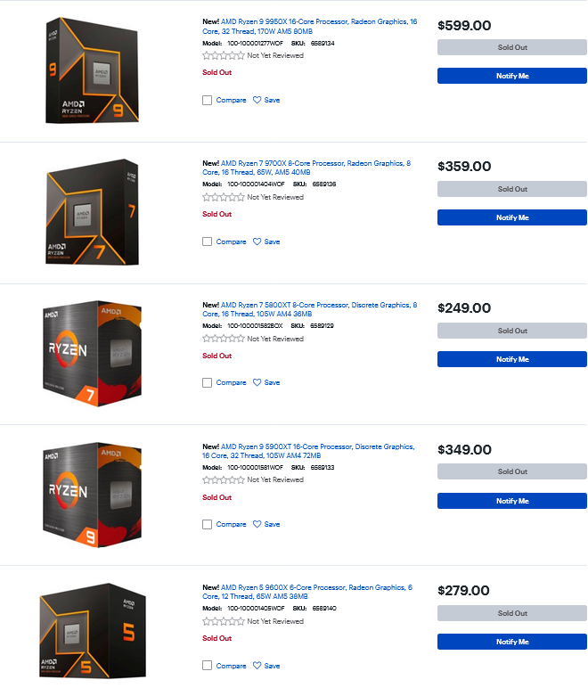
Although AMD delayed launch of its Ryzen 9000-series processors based on the Zen 5 microarchitecture from July 31, to early and mid-August, the company's partner (and major US retailer) Best Buy briefly began listing the new CPUs today, revealing a very plausible set of launch prices. As per the retailer's product catalog, the most affordable unlocked Zen 5-based processor will cost $279, whereas the highest-performing Zen 5-powered CPU will cost $599 at launch.
AMD will start its Ryzen 9000 series rollout from relatively inexpensive six-core Ryzen 5 9600X and eight-core Ryzen 7 9700X on August 8. Per the Best Buy listing, the Ryzen 5 9600X will cost $279, whereas the Ryzen 7 9700X will carry a recommended price tag of $359. Meanwhile, The more advanced 12-core Ryzen 9 9900X and 16-core Ryzen 9 9950X will hit the market on August 15 at MSRPs of $449 and $599, respectively, based on the Best Buy listing.
AMD Ryzen 9000 Series Processors Zen 5 Microarchitecture (Granite Ridge) AnandTech Cores / Threads Base Freq Turbo Freq L2 Cache L3 Cache TDP MSRP Ryzen 9 9950X 16C / 32T 4.3GHz 5.7GHz 16 MB 64 MB 170 W $599 Ryzen 9 9900X 12C / 24T 4.4GHz 5.6GHz 12 MB 64 MB 120 W $359 Ryzen 7 9700X 8C / 16T 3.8GHz 5.5GHz 8 MB 32 MB 65 W $449 Ryzen 5 9600X 6C / 12T 3.9GHz 5.4GHz 6 MB 32 MB 65 W $279It is noteworthy that when compared to the launch prices of the Zen 4-based Ryzen 7000 processors, the new Zen 5-powered Ryzen 9000 CPUs come in cheaper. The range topping Ryzen 9 5950X started at $799 in 2020, while the Ryzen 9 7950X had a recommended $699 price tag in 2022. By contrast, the top-end Ryzen 9 9950X is listed at $599. Both Ryzen 7 5600X and Ryzen 7 7600X cost $299 at launch, while the upcoming Ryzen 5 9600X will apparently be priced at $279 at launch.
As always with accidental retailer listings, it should be emphasized that AMD has not yet announced official pricing for their Ryzen 9000 CPUs. Given Best Buy's status as one of the largest US electronics retailers, these prices carry a very high probability of being accurate; but none the less, they should be taken with a grain of salt – if only because last-minute price changes are not unheard of with new CPU launches.
Source: Best Buy (via @momomo_us)
Micron Ships Denser & Faster 276 Layer TLC NAND, Arriving First In Micron 2650 Client SSDs
Published: Jul 31nd 2024 11:15am on AnandTech
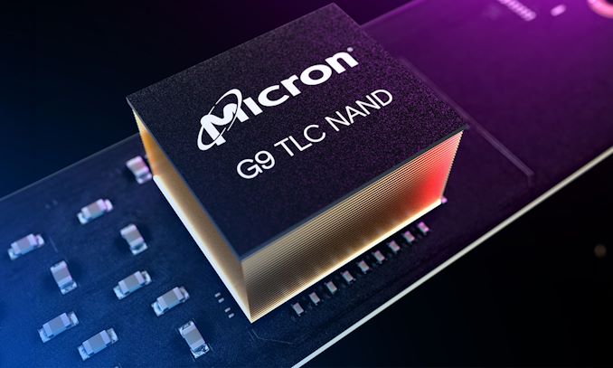
Micron on Tuesday announced that the company has begun shipping its 9th Generation (G9) 276 layer TLC NAND. The next generation of NAND from the prolific memory maker, Micron's latest NAND is designed to further push the envelope on TLC NAND performance, offering significant density and performance improvements over its existing NAND technology.
Micron's G9 TLC NAND memory features 276 active layers, which is up from 232-layers in case of Micron's previous generation TLC NAND. At this point the company is being light on technical details in their official material. However in a brief interview with Blocks & Files, the company confirmed that their 276L NAND still uses a six plane architecture, which was first introduced with the 232L generation. At this point we're assuming Micron is also string-stacking two decks of NAND together, as they have been for the past couple of generations, which means we're looking at 138 layer decks.
Micron TLC NAND Flash Memory 276L 232L (B58R) 176L (B47R) Layers 276 232 176 Decks 2 (x138)? 2 (x116) 2 (x88) Die Capacity 1 Tbit 1 Tbit 512 Gbit Die Size (mm2) ~48.9mm2 ~70.1mm2 ~49.8mm2 Density (Gbit/mm2) ~21 14.6 10.3 I/O Speed 3.6 GT/s (ONFi 5.1) 2.4 GT/s (ONFi 5.0) 1.6 GT/s (ONFI 4.2) Planes 6 6 4 CuA / PuC Yes Yes YesOn the density front, Micron told Blocks & Files that they have improved their NAND density by 44% over their 232L generation. Which, given what we know about that generation, would put the density at around 21 Gbit/mm2. Or for a 1Tbit die of TLC NAND, that works out to a die size of roughly 48.9mm2, comparable to the die size of a 512Gbit TLC die from Micron's older 176L NAND.
Besides improving density, the other big push with Micron's newest generation of NAND was further improving its throughput. While the company's 232L NAND was built against the ONFi 5.0 specification, which topped out at transfer rates of 2400 MT/sec, their new 276L NAND can hit 3600 MT/sec, which is consistent with the ONFi 5.1 spec.
Meanwhile, the eagle-eyed will likely also pick up on Micron's ninth-generation/G9 branding, which is new to the company. Micron's has not previously used this kind of generational branding for their NAND, which up until now has simply been identified by its layer count (and before the 3D era, its feature size). Internally, this is believed to be Micron's 7th generation 3D NAND architecture. However, taking a page from the logic fab industry, Micron seems to be branding it as ninth-generation in order to keep generational parity with its competitors, who are preparing their own 8th/9th generation NAND (and thus cliam that they are the first NAND maker to ship 9th gen NAND).
And while this NAND will eventually end up in all sorts of devices – including, no doubt, high-end PCIe Gen5 drives thanks to its high transfer rates – Micron's launch vehicle for the NAND is their own Micron 2650 client SSD. The 2650 is a relatively straightforward PCIe Gen4 x4 SSD, using an unnamed, DRAMless controller alongside Micron's new NAND. The company is offering it in 3 form factors – M.2 2280, 2242, and 2230 – with a modest set of capacities ranging from 256GB to 1TB.
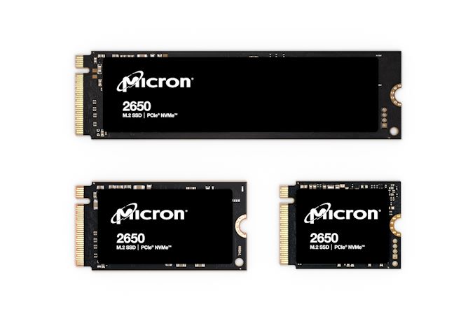
Micron's 2650 NVMe SSDs offer sequential read performance of up to 7000 MB/s as well as sequential write performance of up to 6000 MB/s. As for random performance, we are talking about up to a million of read and write IOPS, depending on configuration.
Micron 2650 SSD Specifications Capacity 1 TB 512 GB 256 GB Controller Micron PCIe Gen4 DRAMless NAND Flash Micron G9 (276L) TLC NAND Form-Factor, Interface Single-Sided M.2-2280/2242/2230 PCIe 4.0 x4, NVMe 1.4c Sequential Read 7000 MB/s 7000 MB/s 5000 MB/s Sequential Write 6000 MB/s 4800 MB/s 2500 MB/s Random Read IOPS 1000K 740K 370K Random Write IOPS 1000K 1000K 500K SLC Caching Yes TCG Opal Encryption 2.02 Write Endurance 600 TBW 300 TBW 200 TBW
The performance of the drives scales pretty significantly with capacity, underscoring how much parallelism is needed to keep up with the PCIe Gen4 controller. The rated capacity of the drives scales similarly, with the smallest drive rated for 200TBW (800 drive writes), while the largest drive is rated for 600 TBW (600 drive writes).
“The shipment of Micron G9 NAND is a testament to Micron’s prowess in process technology and design innovations,” said Scott DeBoer, executive vice president of Technology and Products at Micron. “Micron G9 NAND is up to 73% denser than competitive technologies in the market today, allowing for more compact and efficient storage solutions that benefit both consumers and businesses.”
Micron's G9 276-layer TLC NAND memory is also in qualification with customers in component form, so expect the company's partners to adopt it for their high-end SSDs in the coming quarters. In addition, Micron plans Crucial-branded SSDs based on its G9 NAND memory..
The Cooler Master V Platinum V2 1600W ATX 3.1 PSU Review: Quiet Giant
Published: Jul 31nd 2024 10:00am on AnandTech
Continuing our ongoing look at the latest-generation ATX 3.1 power supplies, today we are examining Cooler Master's V Platinum 1600 V2, a recent addition to the company's expansive PSU lineup.
The V Platinum 1600 V2 is designed to cater to top-end gaming and workstation PCs while offering maximum compatibility with modern ATX directives. And while it boasts a massive 1600 Watt output and a long list of features, the V is a workhorse of a power supply rather than a flagship; Cooler Master is aiming the PSU at budget-conscious users who can't justify spending top dollar, but whom none the less need a powerful and relatively efficient (80PLUS Platinum) power supply.
So often we see PSU vendors go for broke on their high-wattage units, since there's a lot of overlap there with the premium market, so it will be interesting to see what Cooler Master can do with a slightly more modest bill of materials.