Western Digital Previews M.2 2280 PCIe 5.0 x4 NVMe Client SSDs
Published: Aug 8nd 2024 12:00am on AnandTech
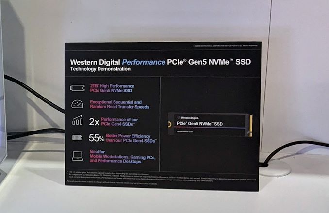
Western Digital's FMS 2024 demonstrations included a preview of their upcoming PCIe 5.0 x4 M.2 2280 NVMe SSDs for mobile workstations and consumer desktops. The Gen 5 client SSD market has been dominated by solutions based on Phison's E26 controller. The first generation products launched with slower NAND flash, while the more recent ones have exceeded the 14 GBps barrier by utilizing Micron's 2400 MT/s 232L 3D TLC. Western Digital has been conservative over the last year or so by focusing more on the mainstream / mid-range market in terms of new product introductions (such as the WD Blue SN5000, WD_BLACK SN770M, and the WD Blue SN580). Their SSD lineup is due for an update with Gen 5 drives being sorely missed. The SSDs being demonstrated at FMS 2024 will end up doing just that.
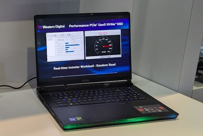
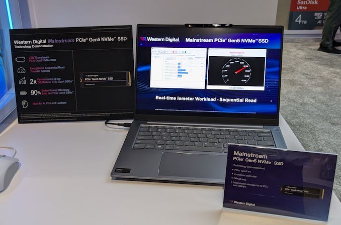
Western Digital's technology demonstrations in this segment involved two different M.2 2280 SSDs - one for the performance segment, and another for the mainstream market. They both utilize in-house controllers - while the performance segment drive uses a 8-channel controller with DRAM for the flash translation layer, the mainstream one utilizes a 4-channel DRAM-less controller. Both drives being benchmarked live were equipped with BiCS8 218-layer 3D TLC.
Western Digital is touting the power efficiency of their platform as a key differentiator, promising south of 7W (performance drive) and 5W (mainstream DRAM-less drive) for the complete SSD under stressful traffic. This makes it suitable for use in mobile workstations, but a good fit for desktops as well.
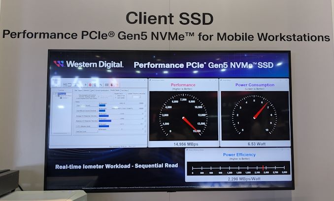
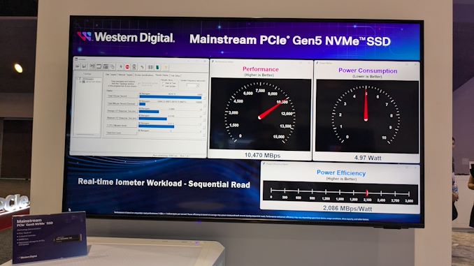
Demonstrated performance numbers indicate almost 15 GBps sequential reads and 2M+ random read IOPS for the performance drive, and 10.7 GBps sequential reads for the mainstream version. Western Digital might have missed the Gen 5 bus as it started out slowly. However, the technology demonstrations with the in-house controller and NAND indicate that WD has caught up just as the Gen 5 market is about to take off.|
Imec Successfully Demonstrates High-NA Lithography for Logic and DRAM Patterning for First Time
Published: Aug 8nd 2024 10:00am on AnandTech
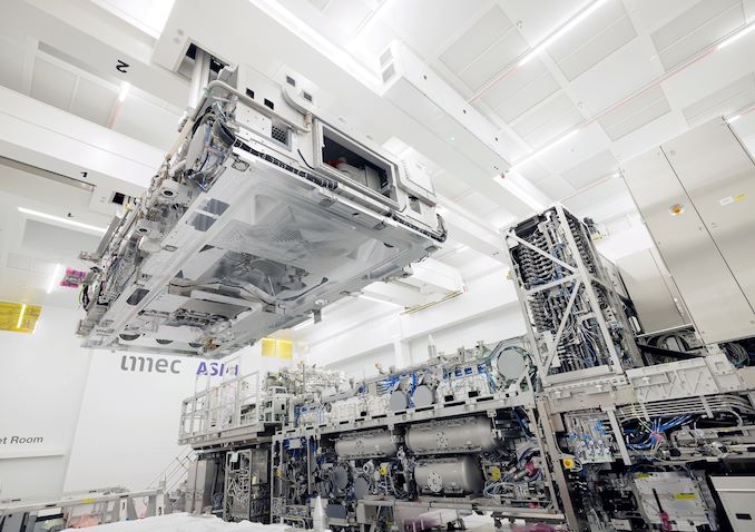
Imec and ASML have announced that the two companies have printed the first logic and DRAM patterns using ASML's experimental Twinscan EXE:5000 EUV lithography tool, the industry's first High-NA EUV scanner. The lithography system achieved resolution that is good enough for 1.4nm-class process technology with just one exposure, which confirms the capabilities of the system and that development of the High-NA ecosystem remains on-track for use in commercial chip production later this decade.
"The results confirm the long-predicted resolution capability of High NA EUV lithography, targeting sub 20nm pitch metal layers in one single exposure," said Luc Van den hove, president and CEO of imec. "High NA EUV will therefore be highly instrumental to continue the dimensional scaling of logic and memory technologies, one of the key pillars to push the roadmaps deep into the ‘angstrom era'. These early demonstrations were only possible thanks to the set-up of the joint ASML-imec lab allowing our partners to accelerate the introduction of High NA lithography into manufacturing."
The successful test printing comes after ASML and Imec have spent the last several months laying the groundwork for the test. Besides the years required to build the complex scanner itself, engineers from ASML, Imec, and their partners needed to develop newer photoresists, underlayers, and reticles. Then they had to take an existing production node and tune it for High-NA EUV tools, including doing optical proximity correction (OPC) and tuning etching processes.
The culmination of these efforts was that, using ASML's pre-production Twinscan EXE:5000 system, Imec was able to successfully pattern random logic structures with 9.5nm dense metal lines, which corresponds to a 19nm pitch and sub-20nm tip-to-tip dimensions. Similarly, Imec also set new high marks in feature density in other respects, including patterning of 2D features at a 22nm pitch, and printing random vias with a 30nm center-to-center distance, demonstrating high pattern fidelity and critical dimension uniformity.
The overall result is that Imec's experiments have proven that ASML's High-NA scanner is delivering on its intended capabilities, printing features at a fine enough resolution for fabricating logic on a 1.4nm-class process technology – and all with a single exposure. The latter is perhaps the most important aspect of this tooling, as the high cost and complexity of the High-NA tool itself (said to be around $400 million) is intended to be offset by being able to return to single-patterning, which allows for higher tool productivity and fewer steps overall.
Imec hasn't just been printing logic structures, either; the group successfully patterned DRAM designs as well, printing both a storage node landing pad alongside the bit line periphery for memory in a single exposure. As with their logic tests, this would allow DRAM designs to be printed in just one exposure, reducing cycle times and eventually costs.
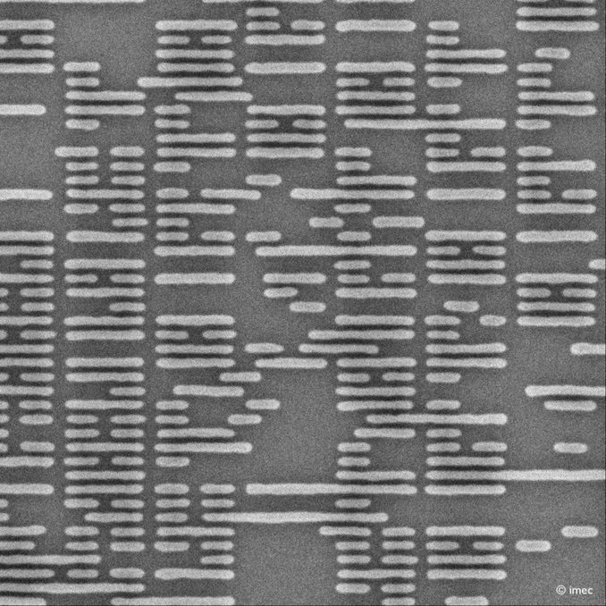 9,5nm random logic structure (19nm pitch) after pattern transfer
Gallery: imec High-NA Pattern Samples


"We are thrilled to demonstrate the world's first High NA-enabled logic and memory patterning in the joint ASML-imec lab as an initial validation of industry applications," said Steven Scheer, senior vice president of compute technologies & systems/compute system scaling at imec. "The results showcase the unique potential for High NA EUV to enable single-print imaging of aggressively-scaled 2D features, improving design flexibility as well as reducing patterning cost and complexity. Looking ahead, we expect to provide valuable insights to our patterning ecosystem partners, supporting them in further maturing High NA EUV specific materials and equipment."
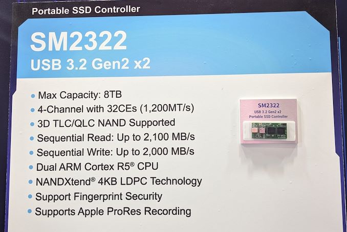
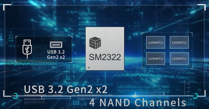
Silicon Motion SM2322 USB 3.2 Gen 2x2 Native Controller: Extended QLC Support for 8 TB PSSDs
Published: Aug 8nd 2024 8:00am on AnandTech
Silicon Motion's SM2320 native USB 3.2 Gen 2x2 controller for USB flash drives and portable SSDs has enjoyed great market success with a large number of design wins over the last few years. Silicon Motion proudly displayed a selection of products based on the SM2320 on the show floor at FMS 2024.
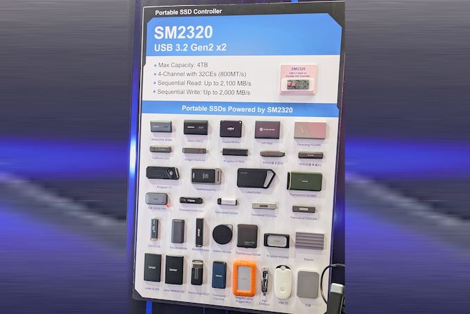
The SM2320 went into mass production in Q3 2021. Since then, the NAND flash market has seen considerable change. QLC is becoming more and more reliable and common, leading to the launch of high-capacity cost-effective 4 TB and 8 TB SSDs. Newer NAND generations with flash operating at higher speeds have also made an appearance.
The SM2320, fabricated in TSMC's 28nm node, supported four channels of NAND flash running at up to 800 MT/s. The new SM2322 uses the same process node and retains support for the same number of flash channels and chip enables (8 CEs per channel). However, the NAND can now operate at up to 1200 MT/s.
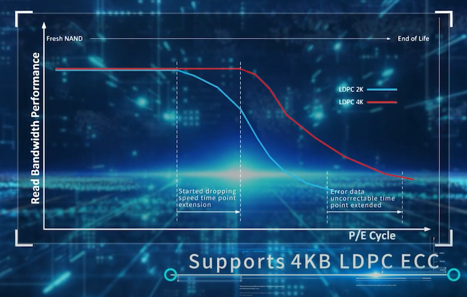
The SM2322 also improves the QLC support, thanks to the implementation of a better ECC scheme. While the SM2320 opted for a 2KB LDPC implementation, the SM2322 goes in for a 4KB LDPC solution. The use of a larger region enables extension of the NAND's useful life.
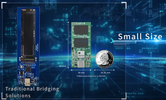
The SM2322 and SM2320 packages are similar in size, and Silicon Motion expects PSSD designs using the SM2320 to adopt the SM2322 with different NAND (higher capacity / speeds) using the same enclosure. Products based on the SM2322 are expected to appear in the market before the end of the year.
Gallery: Silicon Motion SM2322 USB 3.2 Gen 2x2 Native Controller: Extended QLC Support for 8 TB PSSDs


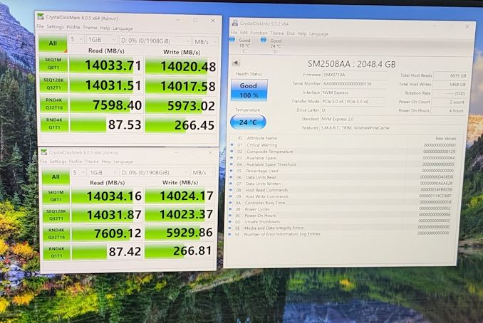
Silicon Motion SM2508 PCIe 5.0 x4 NVMe SSD Controller Set for Mass Production
Published: Aug 7nd 2024 5:00am on AnandTech
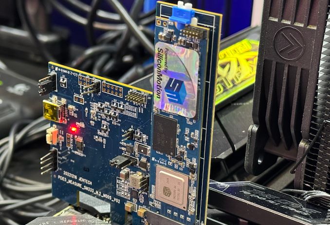
Silicon Motion has been teasing their SM2508 client SSD controller for more than a year now at various trade shows. The controller is finally set for mass production, just in time as the mainstream segment of the Gen 5 SSD market is poised to take off. Silicon Motion expects SSDs based on the SM2508 to be available for purchase by the end of the year.
At FMS 2024, the company was reusing the same information cards seen at Computex in June. The specifications of the SM2508 from our Computex coverage are reproduced here.
Silicon Motion NVMe Client SSD Controller Comparison SM2508 SM2264 SM2268XT2 SM2269XT Market Segment High-End Mainstream Manufacturing Process 6nm 12nm 12nm 12nm CPU Cores 4x Cortex R8 4x Cortex R8 2x Cortex R8 2x Cortex R8 Error Correction 4K+ LDPC 4K LDPC 4K+ LDPC 4K LDPC DRAM DDR4, LPDDR4X DDR4, LPDDR4X No No Host Interface PCIe 5.0 x4 PCIe 4.0 x4 PCIe 4.0 x4 PCIe 4.0 x4 NVMe Version NVMe 2.0 NVMe 1.4 NVMe 2.0 NVMe 1.4 NAND Channels, Interface Speed 8 ch, 3600 MT/s 8 ch, 1600 MT/s 4 ch, 3600 MT/s 4 ch, 1600 MT/s Sequential Read 14.5 GB/s 7.5 GB/s 7.4 GB/s 5.1 GB/s Sequential Write 14 GB/s 7 GB/s 6.7 GB/s 4.8 GB/s 4KB Random Read IOPS 2500k 1300k 1200k 900k 4KB Random Write IOPS 2500k 1200k 1200k 900kCurrent Gen 5 SSDs in the consumer client market are currently all based on Phison's E26 controller. The appearance of newer platform solutions for SSD vendors is bound to be good from both an end-user pricing and adoption perspective.
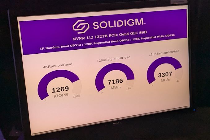
Solidigm 122 TB Enterprise QLC SSD Announced for Early 2025 Release
Published: Aug 7nd 2024 3:30am on AnandTech
Solidigm's D5-P5336 61.44 TB enterprise QLC SSD released in mid-2023 has seen unprecedented demand over the last few quarters, driven by the insatiable demand for high-capacity storage in AI datacenters. Multiple vendors have recognized and started preparing products to service this demand, but Solidigm appears to have taken the lead in actual market availability.
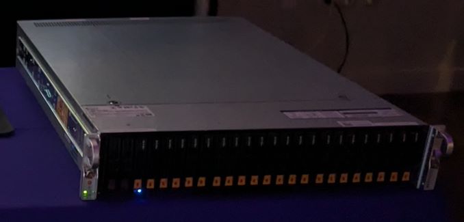
At FMS 2024, Solidigm previewed a U.2 version of their upcoming 122 TB enterprise QLC SSD. The proof-of-concept Gen 4 drives were running live in a 2U server, and Solidigm is preparing them for an early 2025 release.
Given the capacity play, Solidigm will be relying on QLC technology. However, the company was coy about confirming the NAND generation used in the product.
 Source: The Advantages of Floating Gate Technology (YouTube)
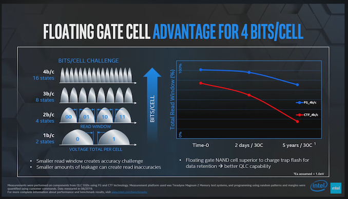
The 61.44 TB D5-P5336 currently utilizes Solidigm's 192L 3D QLC based on the floating gate architecture. This has a distinct advantage for QLC endurance compared to the charge trap architecture also available to Solidigm from SK hynix. That said, SK hynix's 238L NAND also has a QLC avatar, which gives Solidigm the flexibility to use either NAND for the production version of the 122 TB drive. Solidigm expects to confirm this by the end of year in preparation for volume shipment in the first half of 2025.
Corsair Transitions to Cybenetics Certification for Power Supplies
Published: Aug 7nd 2024 2:00am on AnandTech
Corsair, a prominent figure in PC components, has announced a strategic shift in its approach to power supply unit (PSU) certifications. The company is dropping the widely recognized 80 PLUS certification in favor of the newer but more comprehensive Cybenetics certification.
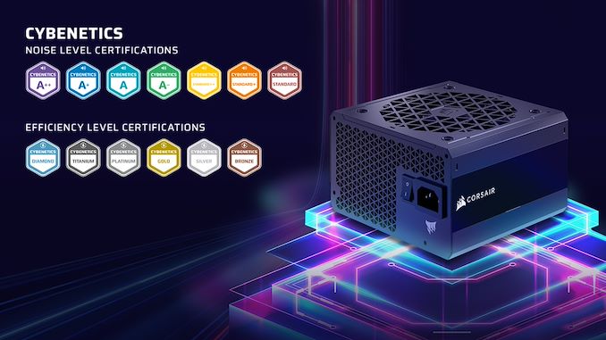
According to the press release, the primary reason for Corsair’s move to Cybenetics certifications lies in the program's dual focus on both energy efficiency and noise levels. While the 80 PLUS certification has been a standard in the industry for decades, it exclusively measures energy conversion efficiency at four load levels (10%, 20%, 50%, 100%). Despite its long-standing presence, the 80 PLUS program has not seen significant updates in over 15 years, which limits its ability to provide a holistic view of PSU performance.
On the other hand, Cybenetics offers a more nuanced approach. It evaluates PSUs across multiple load levels and includes noise level assessments. This dual certification system rates efficiency on a familiar scale (Bronze to Titanium, plus a higher certification called Diamond) and noise levels from Standard (noisy) to A++ (virtually silent). By incorporating noise measurements, Cybenetics provides a more comprehensive overview of PSU performance, addressing an important aspect often overlooked by other certification programs. Cybenetics also enforces Power Factor, 5VSB efficiency, and Vampire Power thresholds, all important to the overall efficiency of a PSU.
Even though they're dropping 80 PLUS in favor of Cybernetics, Corsair is being highly diplomatic with their press release. They even suggest that the reader should not disregard either in favor of the other.
Our opinion is a bit harsher: the simplicity of the 80 PLUS certification program has led to two major flaws. First, manufacturers have primarily focused on maximizing efficiency at three specific load points, neglecting overall performance. Second, the majority of PSUs have clustered around the 80 PLUS Gold and Platinum certifications, with very few achieving the stringent Titanium level. This results in hundreds of PSUs with significantly different technical capabilities sharing the same certification badge, creating a misleading uniformity that fails to reflect true performance disparities.
Furthermore, almost every PSU platform that has been released over the past 15 years would achieve 80Plus Gold status or greater, with very few products falling down to the 80Plus Bronze certification and almost zero meeting the 80Plus White and 80Plus Silver requirements, making the three lowermost certifications practically defunct. Cybenetics dual certification certainly does not solve every issue and cannot fully assess everything there is to assess about a PSU, but it certainly makes much more information available to the user and allows users to at least factor in acoustics performance when purchasing a product.
The issue that seems to remain is that, due to the slackest requirements, manufacturers were almost always certifying their units with an input voltage of 115 VAC, resulting in myriads of units carrying a certification badge that would fail the same 80Plus certification requirements with an input voltage of 230 VAC. Unfortunately, this is also true for the Cybenetics standard, as the badges do not inform the user about the input voltage that the certification was attained with. However, as the Cybenetics standard revolves around average efficiency and not efficiency at specific load points, the majority of the PSUs should meet both efficiency thresholds and not the other way around.
Certification processes can be costly for manufacturers. By opting for the Cybenetics program, Corsair possibly aims to get the most value from its certification investments. Cybenetics offers more detailed and up-to-date testing methodologies, ensuring that the data provided is more reflective of real-world usage scenarios. In any case, Corsair’s shift to Cybenetics certification marks a significant development in the evaluation of PSUs and has the potential to create waves in the market.
Ultimately, this move has the potential disrupt the status quo. With Corsair's sheer size and influence in the larger power supply market, this could very well prompt other manufacturers to follow suit, and possibly even reshape consumer expectations and benchmarks for PSU quality.
AMD Launches New Ryzen & Radeon Gaming Bundle: Warhammer 40,000: Space Marine 2 and Unknown 9: Awakening
Published: Aug 7nd 2024 12:30am on AnandTech

AMD has made itself quite a reputation with its bundling campaigns over the years, and every new season we can be sure that the company will be giving away free games with the purchase of its hardware. This summer will certainly not be exception as AMD will be bundling Warhammer 40,000: Space Marine 2 and Unknown 9: Awakening titles with its Ryzen 7000 CPUs and Radeon RX 7000 video cards.
The latest bundle offer essentially covers all of AMD's existing mid-range and high-end consumer desktop products, sans the to-be-launched Ryzen 9000 series. That includes not only AMD's desktop parts, such as the Ryzen 9 7800X3D, but also virtually their entire stack of Radeon RX 7000 video cards, right on down to the 7600 XT.
AMD's laptop hardware is also covered as well, which is a much rarer occurence. Mid-range and high-end Ryzen 7000 mobile parts are part of the game bundle, including the 7940HS and even the 7435HS. However the refreshed version of these parts, sold under the Ryzen 8000 Mobile line, are not. Meanwhile systems with a Radeon RX 7700S or 7600S mobile GPU are included as well.
This deal is available only through participating retailers (in case of the U.S. and Canada these are Amazon and Newegg). The promotion is also applicable to select laptops containing these components.
AMD's Summer 2024 Ryzen & Radeon Game Bundle (Warhammer 40,000: Space Marine 2 & Unknown 9: Awakening) CPU GPU Desktop Ryzen 9 7950X3D Ryzen 9 7950X Ryzen 9 7900X3D Ryzen 9 7900X Ryzen 9 7900* Ryzen 7 7800X3D* Ryzen 7 7700X* Ryzen 7 7700* Radeon RX 7900 XTX Radeon RX 7900 XT Radeon RX 7900 GRE Radeon RX 7800 XT* Radeon RX 7700 XT* Radeon RX 7600 XT* Laptop Ryzen 9 7940HS Ryzen 7 7840HS Ryzen 7 7735HS Ryzen 7 7435HS Radeon RX 7700S Radeon RX 7600S *This product does not qualify for the promotion in JapanWarhammer 40,000: Space Marine 2 carries an MSRP of $60, whereas the Unknown 9: Awakening is set at $50, so this offer provides an estimated value of $110. The deal is particularly appealing to gamers and those interested in action titles. Meanwhile, fans of such games probably already have AMD's Ryzen 7000 and Radeon RX 7000-series products, so while the deal will be appealing to some users, it may not be appealing for gamers looking to upgrade to AMD's latest Zen 5-powered CPUs.
The campaign starts on August 6, 2024, at 9:00 AM ET and ends on October 5, 2024, at 11:59 PM ET, or when all Coupon Codes are claimed, whichever happens first. Coupon Codes must be redeemed by November 2, 2024, at 11:59 PM ET.
Western Digital Teases 128 TB Enterprise SSD: BiCS8 3D QLC for AI Workloads
Published: Aug 7nd 2024 11:00am on AnandTech
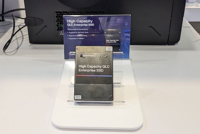
A week after Western Digital confirmed that it had begun sampling of its 64 TB SSDs for datacenters, the company has teased its next-generation product, a 128 TB solid-state drive at FMS 2024.
For now, all we know about Western Digital's 128 TB SSD is that it uses the company's BiCS8 QLC NAND memory and is designed primarily for 'fast AI data lakes and capacity-intensive performance applications,' as Western Digital does not seem to be disclosing too much information about its upcoming product. The sample on the show floor indicates the usage of a U.2/U.3 form-factor suitable for GPU servers.
BiCS8 NAND has 218 layers and uses a hybrid bonding scheme that is being tagged as CMOS directly bonded to Array (CBA). It must be noted that this technique is an evolutionary successor to Micron's CMOS-under-Array (CuA) and SK hynix's Periphery-under-Cell (4D PUC) technologies. BiCS8 NAND can interface to the controller at rates of up to 3600 MT/s, making it suitable for Gen 4+ drives.
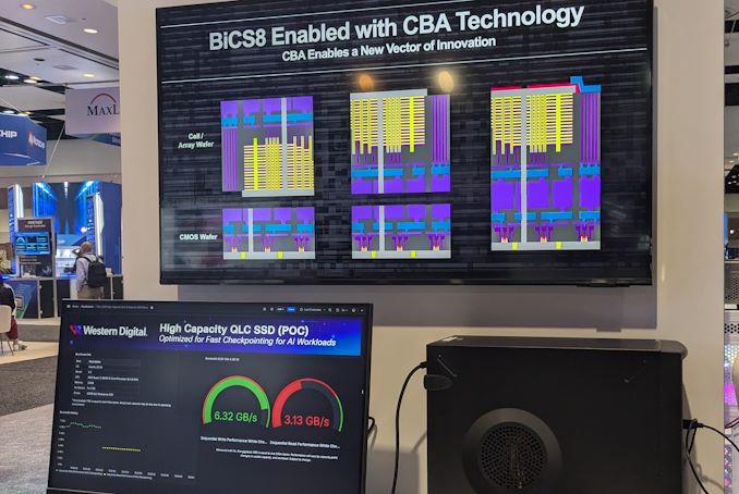
The technology demonstration on the show floor had the drive's firmware optimized for AI checkpointing - a workload that involves sequential writes, but also requires the drive to support a minimum QoS for simultaneous read operations.
Western Digital is not the only company to talk about high-performance 128 TB SSDs. Samsung recently said that it has technology to build 120 TB-class drives, and Solidigm was also demonstrating a proof-of-concept 122 TB QLC SSD at FMS 2024. AI workloads have triggered an insatiable need for dense and power-efficient storage in the data center. This has served as an impetus for enterprise SSD vendors to continue pushing the envelop on the per-drive capacity front.
The AMD Ryzen 7 9700X and Ryzen 5 9600X Review: Zen 5 is Alive
Published: Aug 7nd 2024 9:00am on AnandTech
Last month, AMD launched their first processors using the Zen 5 microarchitecture for the mobile market via their Ryzen AI 300 series. Typically, with AMD Ryzen launches, we usually see the desktop parts come first, with the flagship model and then the mobile coming after. This time around, AMD has changed the dynamic of their release schedule with Zen 5 by launching the mobile chips first, which includes the Ryen AI 9 HX 370, which we reviewed last month. Today, Zen 5 on desktop has its turn, as AMD has launched two mid-range desktop processors, the Ryzen 7 9700X and the Ryzen 5 9600X.
AMD has launched two of the four announced Ryzen 9000 series processors today. The entry-level model is the Ryzen 5 9600X, a 6C/12T part with full-sized Zen 5 cores that can boost up to 5.4 GHz out of the box. The other model launched today is the Ryzen 7 9700X, which also features 8C/16T of Zen 5 and a boost clock speed of up to 5.5 GHz.
As part of AMD's push on platform longevity, the Ryzen 9000 series shares the same AM5 socket as its predecessor, meaning users can use X670E/X670 and B650E/B650 motherboards with a firmware update. We expected to see the newer X870X motherboards come with the Ryzen 9000 release, but unfortunately, these have been delayed.
So now we have Zen 5 in the form of the Ryzen 9000 series finally hitting the desktop, sans the top two SKUs, the Ryzen 9 9950X and Ryzen 9 9900X, which are coming later, it's time to see how much of an improvement Zen 5 is over Zen 4, not just in single-threaded but also multi-threaded workloads as AMD has promised up to an uplift of16% IPC on average. Both the Ryzen 7 9700X and Ryzen 5 9600X have a TDP of 65 W, which we see as more aligned with the non-X SKUs, so it will be interesting to see how Zen 5 performs in terms of both performance and efficiency.
Intel 18A Status Update: First Chips Booting, First External Customer Tape-Out in H1’25
Published: Aug 6nd 2024 11:01am on AnandTech
Following Intel’s painful Q2 earnings call and the announcement of their 2025 cost reduction plan last week, it has become increasingly evident that Intel’s future is in the hands of their foundry group. Between Intel’s IDM 2.0 initiative and their internal chip production plans, all roads lead back to Intel retaking – and retaining – fab process leadership. To win as both a chip designer and a contract chip maker, Intel needs to be able to regain the fab technology lead it once held. In many respects it’s a return to Intel’s classic (and most successful) operating model, but never has it been so risky at it is for the already weakened Intel.
Intel’s do-or-die dash for process leadership means that, for the next 18 months or so, all eyes are on the company’s 20A and 18A process nodes. The final nodes in their ambitious 5 Nodes in 4 Years roadmap, the twinned 20A/18A are the culmination of several new technologies, primarily Intel’s GAAFET implementation (RibbonFET), which is being combined with PowerVia, Intel’s backside power delivery network (BS-PDN) technology. 20A is set to serve as Intel’s early version of the node, and 18A the refined version for long-term use both internally, and as the first major external node for Intel Foundry. To say that everything rides on Intel 18A isn’t quite accurate, but it’s only a slight embellishment.
To that end, we’re going to see Intel deliver a lot of status updates on 18A over the next year as they continue to outline to investors and external customers alike that they have the manufacturing side of their business in order. And today is one of those days, with a fresh update on the state of 18A.
18A Chips Back & BootingSo what’s new with 18A? The biggest news out of Intel this morning is that their first 18A chips are back from the development fab and are successfully booting operating systems. This means the silicon not only works (power-on), but works well enough to complete core tasks. It’s a major step in bringing up a chip, and at this point, Intel wants to make sure to let the whole world know.
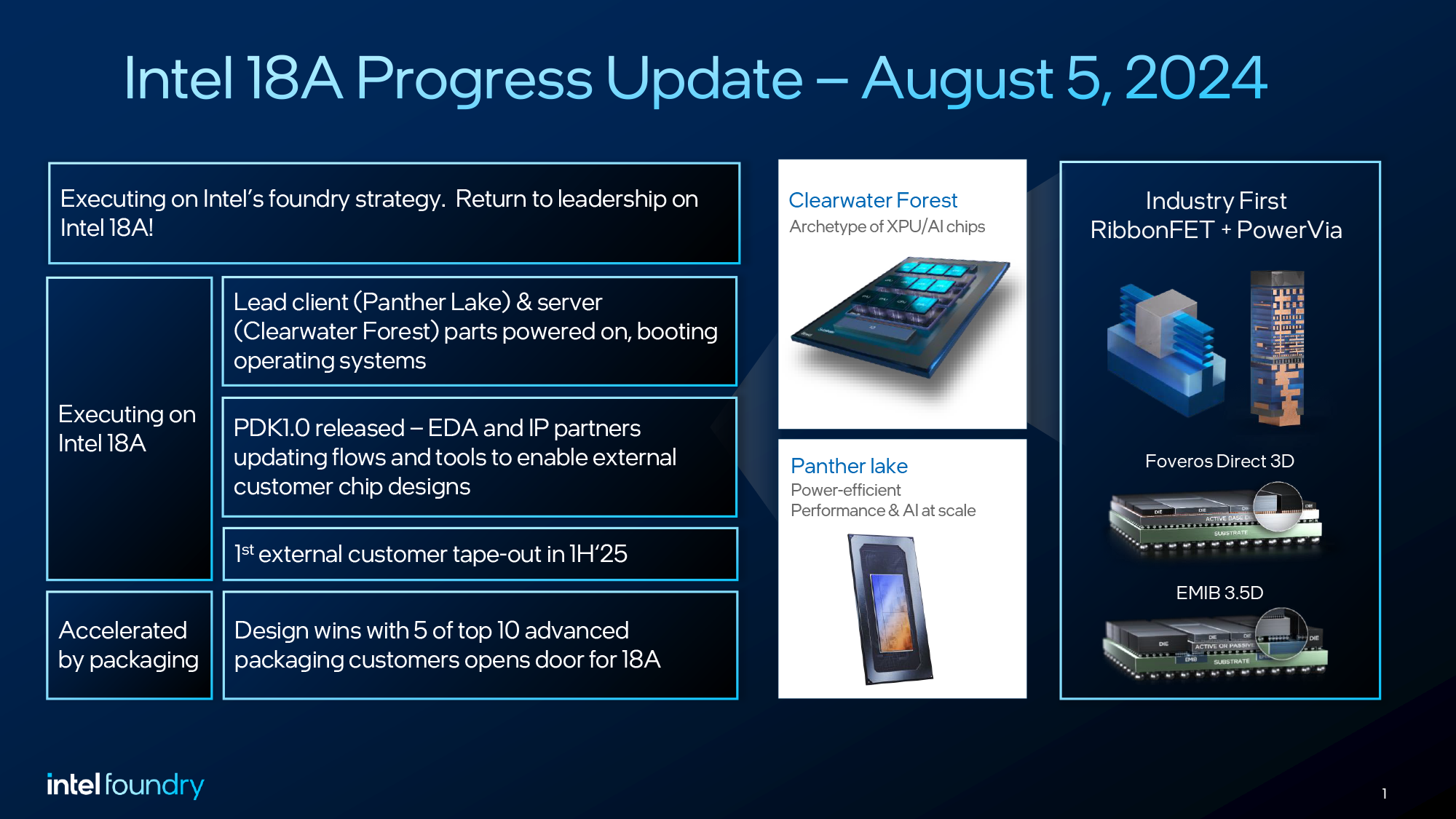
Earlier this year the company finished taping out both of its lead 18A chips: Panther Lake for clients, and Clearwater Forest for servers. And it’s both chips that are booting. This is made all the more significant by the fact that Clearwater Forest also relies on Intel’s die-to-die hybrid bonding packaging technology, Foveros Direct 3D, where it will be the lead product for that technology as well. Which for Intel, is a promising sign that not only are their silicon lithography ambitions paying off, but their intention to lead in advanced packaging is on-track as well.
And while Intel doesn’t normally talk about yields this early in the game, it’s interesting to note that in a separate Q&A being published this morning with Intel Foundry’s new boss, Kevin O’Buckley, the head of Foundry Services explicitly comments that Panther Lake is “yielding well”. Similarly, Panther Lake’s DDR memory controller (a complex block mixing logic with a PHY) is already running at its target frequency. Progress is going so well, apparently, that according to O’Buckley, it’s ahead of schedule on its product qualification milestones.
PDK 1.0 Released, First External Customer Tape-Out Expected in H1’25As for Intel’s contract foundry business, the company is ramping up its efforts there now that the first full process design kit (PDK) is ready for 18A. Intel released their 18A PDK 1.0 last month, giving Intel’s customers (and potential customers) the tools to finally finish designing their chips for production. As is typically the case of a new node, pre-release PDKs were available for companies to get started on their designs, but the 1.0 PDK is typically needed to finish those designs and align them with the formal and finalized process specifications.
For Intel, getting an external PDK out for a leading-edge process node is no small feat, as the company has spent decades operating its fabs for the benefit of its internal product design teams. A useful PDK for external customers – and really, a useful fab environment altogether – not only needs process nodes that stick to their specifications rather than making bespoke adjustments, but it means that Intel needs to document and define all of this in a useful, industry standard fashion. One of the major failings of Intel’s previous efforts to get into the contract foundry business, besides being half-hearted efforts overall, is that they didn’t author PDKs that external companies could easily use. At the end of the day, Intel is looking to woo customers from TSMC and Samsung, and as such Intel needs to provide PDKs that chip designers accustomed to contemporary contract fabs can use.
Those efforts are finally paying off, if slowly. While still not sharing any names, Intel expects their first external customer chip design will tape out in the first half of 2025 (H1’25). And, as Intel hopes, it will be the first of many.
Ultimately, the hard work for Intel foundry is not yet complete, and it will continue from here. With initial 18A development wrapping up, Intel’s needs are no longer just fab R&D, but marketing and customer relations. Which, going back to the start of this article, is why Intel is so keen to release status updates on 18A: it’s part of a broader approach to entice new customers to give Intel a try. Even in the best-case scenario, it will take upwards of a decade to capture a majority of the market for fabbing cutting-edge chips. But Intel has to start that marketing push if they’re going to get there.
In the meantime, if all continues going well for Intel, we should be seeing the first 18A chips released in the latter half of near year.