Rapidus Wants to Offer Fully Automated Packaging for 2nm Fab to Cut Chip Lead Times
Published: Aug 13nd 2024 8:00am on AnandTech
One of the core challenges that Rapidus will face when it kicks off volume production of chips on its 2nm-class process technology in 2027 is lining up customers. With Intel, Samsung, and TSMC all slated to offer their own 2nm-class nodes by that time, Rapidus will need some kind of advantage to attract customers away from its more established rivals. To that end, the company thinks they've found their edge: fully automated packaging that will allow for shorter chip lead times than manned packaging operations.
In an interview with Nikkei, Rapidus' president, Atsuyoshi Koike, outlined the company's vision to use advanced packaging as a competitive edge for the new fab. The Hokkaido facility, which is currently under construction and is expecting to begin equipment installation this December, is already slated to both produce chips and offer advanced packaging services within the same facility, an industry first. But ultimately, Rapidus biggest plan to differentiate itself is by automating the back-end fab processes (chip packaging) to provide significantly faster turnaround times.
Rapidus is targetting back-end production in particular as, compared to front-end (lithography) production, back-end production still heavily relies on human labor. No other advanced packaging fab has fully automated the process thus far, which provides for a degree of flexibility, but slows throughput. But with automation in place to handle this aspect of chip production, Rapidus would be able to increase chip packaging efficiency and speed, which is crucial as chip assembly tasks become more complex. Rapidus is also collaborating with multiple Japanese suppliers to source materials for back-end production.
"In the past, Japanese chipmakers tried to keep their technology development exclusively in-house, which pushed up development costs and made them less competitive," Koike told Nikkei. "[Rapidus plans to] open up technology that should be standardized, bringing down costs, while handling important technology in-house."
Financially, Rapidus faces a significant challenge, needing a total of ¥5 trillion ($35 billion) by the time mass production starts in 2027. The company estimates that ¥2 trillion will be required by 2025 for prototype production. While the Japanese government has provided ¥920 billion in aid, Rapidus still needs to secure substantial funding from private investors.
Due to its lack of track record and experience of chip production as. well as limited visibility for success, Rapidus is finding it difficult to attract private financing. The company is in discussions with the government to make it easier to raise capital, including potential loan guarantees, and is hopeful that new legislation will assist in this effort.
Kioxia Demonstrates RAID Offload Scheme for NVMe Drives
Published: Aug 12nd 2024 2:30am on AnandTech
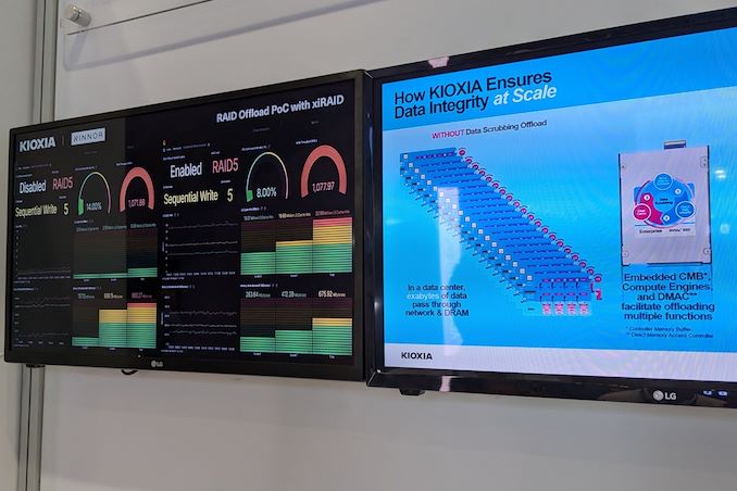
At FMS 2024, Kioxia had a proof-of-concept demonstration of their proposed a new RAID offload methodology for enterprise SSDs. The impetus for this is quite clear: as SSDs get faster in each generation, RAID arrays have a major problem of maintaining (and scaling up) performance. Even in cases where the RAID operations are handled by a dedicated RAID card, a simple write request in, say, a RAID 5 array would involve two reads and two writes to different drives. In cases where there is no hardware acceleration, the data from the reads needs to travel all the way back to the CPU and main memory for further processing before the writes can be done.
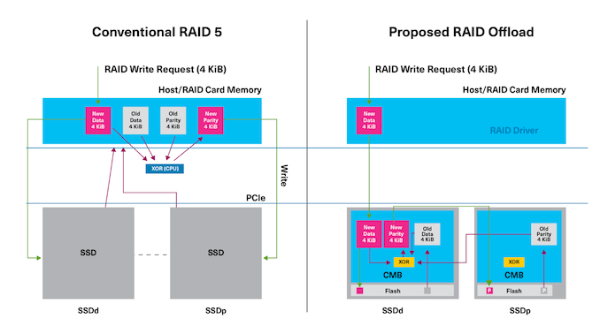
Kioxia has proposed the use of the PCIe direct memory access feature along with the SSD controller's controller memory buffer (CMB) to avoid the movement of data up to the CPU and back. The required parity computation is done by an accelerator block resident within the SSD controller.
In Kioxia's PoC implementation, the DMA engine can access the entire host address space (including the peer SSD's BAR-mapped CMB), allowing it to receive and transfer data as required from neighboring SSDs on the bus. Kioxia noted that their offload PoC saw close to 50% reduction in CPU utilization and upwards of 90% reduction in system DRAM utilization compared to software RAID done on the CPU. The proposed offload scheme can also handle scrubbing operations without taking up the host CPU cycles for the parity computation task.
Kioxia has already taken steps to contribute these features to the NVM Express working group. If accepted, the proposed offload scheme will be part of a standard that could become widely available across multiple SSD vendors.
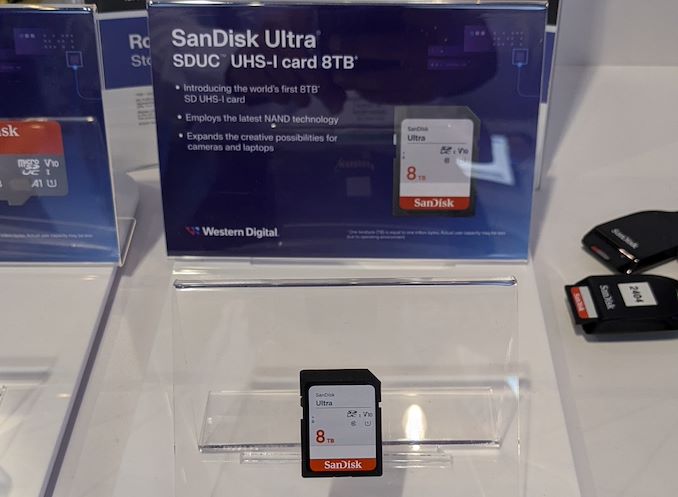
Western Digital Introduces 4 TB microSDUC, 8 TB SDUC, and 16 TB External SSDs
Published: Aug 12nd 2024 1:30am on AnandTech
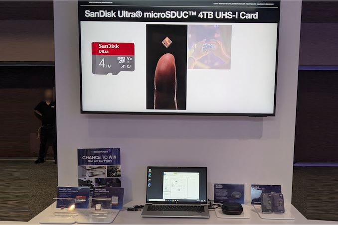
Western Digital's BiCS8 218-layer 3D NAND is being put to good use in a wide range of client and enterprise platforms, including WD's upcoming Gen 5 client SSDs and 128 TB-class datacenter SSD. On the external storage front, the company demonstrated four different products: for card-based media, 4 TB microSDUC and 8 TB SDUC cards with UHS-I speeds, and on the portable SSD front we had two 16 TB drives. One will be a SanDisk Desk Drive with external power, and the other in the SanDisk Extreme Pro housing with a lanyard opening in the case.
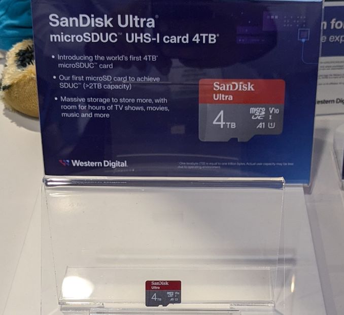
All of these are using BiCS8 QLC NAND, though I did hear booth talk (as I was taking leave) that they were not supposed to divulge the use of QLC in these products. The 4 TB microSDUC and 8 TB SDUC cards are rated for UHS-I speeds. They are being marketed under the SanDisk Ultra branding.
The SanDisk Desk Drive is an external SSD with a 18W power adapter, and it has been in the market for a few months now. Initially launched in capacities up to 8 TB, Western Digital had promised a 16 TB version before the end of the year. It appears that the product is coming to retail quite soon. One aspect to note is that this drive has been using TLC for the SKUs that are currently in the market, so it appears unlikely that the 16 TB version would be QLC. The units (at least up to the 8 TB capacity point) come with two SN850XE drives. Given the recent introduction of the 8 TB SN850X, an 'E' version with tweaked firmware is likely to be present in the 16 TB Desk Drive.
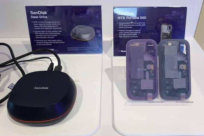
The 16 TB portable SSD in the SanDisk Extreme housing was a technology demonstration. It is definitely the highest capacity bus-powered portable SSD demonstrated by any vendor at any trade show thus far. Given the 16 TB Desk Drive's imminent market introduction, it is just a matter of time before the technology demonstration of the bus-powered version becomes a retail reality.
The Noctua NH-D15 G2 LBC Cooler Review: Notoriously Big, Incredibly Good
Published: Aug 12nd 2024 12:00am on AnandTech
When you buy a retail computer CPU, it usually comes with a standard cooler. However, most enthusiasts find that the stock cooler just does not cut it in terms of performance. So, they often end up getting a more advanced cooler that better suits their needs. Choosing the right cooler isn't a one-size-fits-all deal – it is a bit of a journey. You have to consider what you need, what you want, your budget, and how much space you have in your setup. All these factors come into play when picking out the perfect cooler.
When it comes to high-performance coolers, Noctua is a name that frequently comes up among enthusiasts. Known for their exceptional build quality and superb cooling performance, Noctua coolers have been a favorite in the PC building community for years. A typical Noctua cooler will be punctuated by incredibly quiet fans and top-notch cooling efficiency overall, which has made them ideal for overclockers and builders who want to keep their systems running cool and quiet.
In this review, we'll be taking a closer look at the NH-D15 G2 cooler, the successor to the legendary NH-D15. This cooler comes with a hefty price tag of $150 but promises to deliver the best performance that an air cooler can currently achieve. The NH-D15 G2 is available in three versions: one standard version as well as two specialized variants – LBC (Low Base Convexity) and HBC (High Base Convexity). These variants are designed to make better contact with specific CPUs; the LBC is recommended for AMD AM5 processors, while the HBC is tailored for Intel LGA1700 processors, mirroring the slightly different geometry of their respective heatspeaders. Conversely, the standard version is an “one size fits all” approach for users who care more about long-term compatibility over squeezing out every ounce of potential the cooler has.
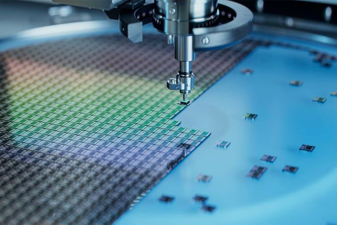
Kioxia Details BiCS 8 NAND at FMS 2024: 216 Layers With Superior Scaling
Published: Aug 12nd 2024 10:00am on AnandTech
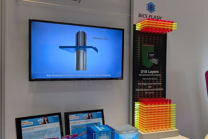
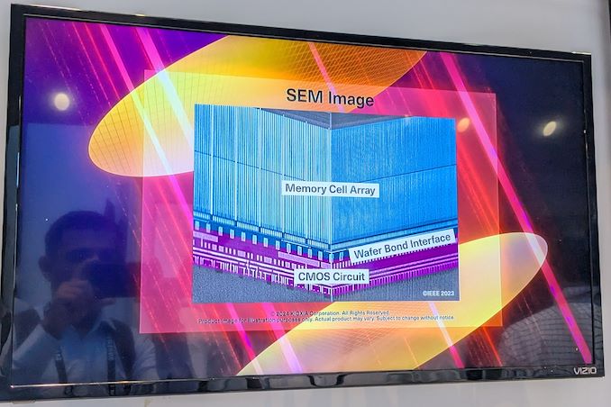
Kioxia's booth at FMS 2024 was a busy one with multiple technology demonstrations keeping visitors occupied. A walk-through of the BiCS 8 manufacturing process was the first to grab my attention. Kioxia and Western Digital announced the sampling of BiCS 8 in March 2023. We had touched briefly upon its CMOS Bonded Array (CBA) scheme in our coverage of Kioxial's 2Tb QLC NAND device and coverage of Western Digital's 128 TB QLC enterprise SSD proof-of-concept demonstration. At Kioxia's booth, we got more insights.
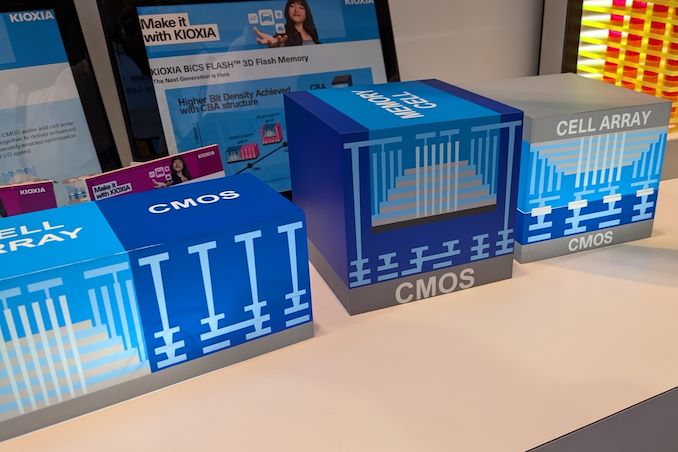
Traditionally, fabrication of flash chips involved placement of the associate logic circuitry (CMOS process) around the periphery of the flash array. The process then moved on to putting the CMOS under the cell array, but the wafer development process was serialized with the CMOS logic getting fabricated first followed by the cell array on top. However, this has some challenges because the cell array requires a high-temperature processing step to ensure higher reliability that can be detrimental to the health of the CMOS logic. Thanks to recent advancements in wafer bonding techniques, the new CBA process allows the CMOS wafer and cell array wafer to be processed independently in parallel and then pieced together, as shown in the models above.
The BiCS 8 3D NAND incorporates 218 layers, compared to 112 layers in BiCS 5 and 162 layers in BiCS 6. The company decided to skip over BiCS 7 (or, rather, it was probably a short-lived generation meant as an internal test vehicle). The generation retains the four-plane charge trap structure of BiCS 6. In its TLC avatar, it is available as a 1 Tbit device. The QLC version is available in two capacities - 1 Tbit and 2 Tbit.
Kioxia also noted that while the number of layers (218) doesn't compare favorably with the latest layer counts from the competition, its lateral scaling / cell shrinkage has enabled it to be competitive in terms of bit density as well as operating speeds (3200 MT/s). For reference, the latest shipping NAND from Micron - the G9 - has 276 layers with a bit density in TLC mode of 21 Gbit/mm2, and operates at up to 3600 MT/s. However, its 232L NAND operates only up to 2400 MT/s and has a bit density of 14.6 Gbit/mm2.
It must be noted that the CBA hybrid bonding process has advantages over the current processes used by other vendors - including Micron's CMOS under array (CuA) and SK hynix's 4D PUC (periphery-under-chip) developed in the late 2010s. It is expected that other NAND vendors will also move eventually to some variant of the hybrid bonding scheme used by Kioxia.
Intel Publishes First Microcode Update for Raptor Lake Stability Issue, BIOSes Going Out Now
Published: Aug 9nd 2024 3:00am on AnandTech
Following Intel’s run of financial woes and Raptor Lake chip stability issues, the company could use some good news on a Friday. And this week they’re delivering just that, with the first version of the eagerly awaited microcode fix for desktop Raptor Lake processors – as well as the first detailed explanation of the underlying issue.
The new microcode release, version 0x129, is Intel’s first stab at addressing the elevated voltage issue that has seemingly been the cause of Raptor Lake processor degradation over the past year and a half. Intel has been investigating the issue all year, and after a slow start, in recent weeks has begun making more significant progress, identifying what they’re calling an “elevated operating voltage” issue in high-TDP desktop Raptor Lake (13th & 14th Generation Core) chips. Back in late July the company was targeting a mid-August release date for a microcode patch to fix (or rather, prevent) the degradation issue, and just ahead of that deadline, Intel has begun shipping the microcode to their motherboard partners.
Even with this new microcode, however, Intel is not done with the stability issue. Intel is still investigating whether it’s possible to improve the stability of already-degraded processors, and the overall tone of Intel’s announcement is very much that of a beta software fix – Intel won’t be submitting this specific microcode revision for distribution via operating system updates, for example. So even if this microcode is successful in stopping ongoing degradation, it seems that Intel hasn’t closed the book on the issue entirely, and that the company is presumably working towards a fix suitable for wider release.
Capping At 1.55v: Elevated Voltages Beget Elevated VoltagesSo just what does the 0x129 microcode update do? In short, it caps the voltage of affected Raptor Lake desktop chips at a still-toasty (but in spec) 1.55v. As noted in Intel’s previous announcements, excessive voltages seem to be at the cause of the issue, so capping voltages at what Intel has determined is the proper limit should prevent future chip damage.
The company’s letter to the community also outlines, for the first time, just what is going on under the hood with degraded chips. Those chips that have already succumbed to the issue from repeated voltage spikes have deteriorated in such a way that the minimum voltage needed to operate the chip – Vmin – has increased beyond Intel’s original specifications. As a result, those chips are no longer getting enough voltage to operate.
Seasoned overclockers will no doubt find that this is a familiar story, as this is one of the ways that overclocked processors degrade over time. In those cases – as it appears to be with the Raptor Lake issue – more voltage is needed to keep a chip stable, particularly in workloads where the voltage to the chip is already sagging.
And while all signs point to this degradation being irreversible (and a lot of RMAs in Intel’s future), there is a ray of hope. If Intel’s analysis is correct that degraded Raptor Lake chips can still operate properly with a higher Vmin voltage, then there is the possibility of saving at least some of these chips, and bringing them back to stability.
This “Vmin shift,” as Intel is calling it, is the company’s next investigative target. According to the company’s letter, they are aiming to provide updates by the “end of August.”
In the meantime, Intel’s eager motherboard partners have already begun releasing BIOSes with the new microcode, with ASUS and MSI even jumping the gun and sending out BIOSes before Intel had a chance to properly announce the microcode. Both vendors are releasing these as beta BIOSes, reflecting the general early nature of the microcode fix itself. And while we expect most users will want to get this microcode in place ASAP to mitigate further damage on affected chips, it would be prudent to treat these beta BIOSes as just that.
Along those lines, as noted earlier, Intel is only distributing the 0x129 microcode via BIOS updates at this time. This microcode will not be coming to other systems via operating system updates. At this point we still expect distribution via OS updates to be the end game for this fix, but for now, Intel isn’t providing a timeline or other guidance for when that might happen. So for PC enthusiasts, at least, a BIOS update is the only way to get it for now.
Performance Impact: Generally Nil – But Not AlwaysFinally, Intel’s message also provides a bit of guidance on the performance impact of the new microcode, based on their internal testing. Previously the company has indicated that they expected no significant performance impact, and based on their expanded testing, by and large this remains the case. However, there are going to be some workloads that suffer from performance regressions as a result.
So far, Intel has found a couple of workloads where they are seeing regressions. This includes PugetBench GPU Effects Score and, on the gaming side of matters, Hitman 3: Dartmoor. Otherwise, virtually everything else Intel has tested, including common benchmarks like Cinebench, and major games, are not showing performance regressions. So the overall outcome of the fix is not quite a spotless recovery, but it’s also not leading to widespread performance losses, either.
As for AnandTech, we’ll be digging into this on our own benchmark suite as time allows. We have one more CPU launch coming up next week, so there’s no shortage of work to be done in the next few days. (Sorry, Gavin!)
Intel’s Full Statement Intel is currently distributing to its OEM/ODM partners a new microcode patch (0x129) for its Intel Core 13th/14th Gen desktop processors which will address incorrect voltage requests to the processor that are causing elevated operating voltage. For all Intel Core 13th/14th Gen desktop processor users: This patch is being distributed via BIOS update and will not be available through operating system updates. Intel is working with its partners to ensure timely validation and rollout of the BIOS update for systems currently in service. Instability Analysis Update – Microcode Background and Performance Implications In addition to extended warranty coverage, Intel has released three mitigations related to the instability issue – commonly experienced as consistent application crashes and repeated hangs – to help stabilize customer systems with Intel Core 13th and 14th gen desktop processors:- Intel default settings to avoid elevated power delivery impact to the processor (May 2024)
- Microcode 0x125 to fix the eTVB issue in i9 processors (June 2024)
- Microcode 0x129 to address elevated voltages (August 2024)
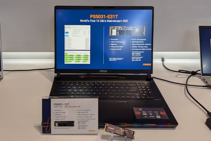
Phison Introduces E29T Gen 4 Controller for Mainstream Client SSDs
Published: Aug 9nd 2024 2:15am on AnandTech

At FMS 2024, Phison gave us the usual updates on their client flash solutions. The E31T Gen 5 mainstream controller has already been seen at a few tradeshows starting with Computex 2023, while the USB4 native flash controller for high-end PSSDs was unveiled at CES 2024. The new solution being demonstrated was the E29T Gen 4 mainstream DRAM-less controller. Phison believes that there is still performance to be eked out on the Gen 4 platform with a low-cost DRAM-less solution.
Phison NVMe SSD Controller Comparison E31T E29T E27T E26 E18 Market Segment Mainstream Consumer High-End Consumer Manufacturing Process 7nm 12nm 12nm 12nm 12nm CPU Cores 2x Cortex R5 1x Cortex R5 1x Cortex R5 2x Cortex R5 3x Cortex R5 Error Correction 7th Gen LDPC 7th Gen LDPC 5th Gen LDPC 5th Gen LDPC 4th Gen LDPC DRAM No No No DDR4, LPDDR4 DDR4 Host Interface PCIe 5.0 x4 PCIe 4.0 x4 PCIe 4.0 x4 PCIe 5.0 x4 PCIe 4.0 x4 NVMe Version NVMe 2.0 NVMe 2.0 NVMe 2.0 NVMe 2.0 NVMe 1.4 NAND Channels, Interface Speed 4 ch, 3600 MT/s 4 ch, 3600 MT/s 4 ch, 3600 MT/s 8 ch, 2400 MT/s 8 ch, 1600 MT/s Max Capacity 8 TB 8 TB 8 TB 8 TB 8 TB Sequential Read 10.8 GB/s 7.4 GB/s 7.4 GB/s 14 GB/s 7.4 GB/s Sequential Write 10.8 GB/s 6.5 GB/s 6.7 GB/s 11.8 GB/s 7.0 GB/s 4KB Random Read IOPS 1500k 1200k 1200k 1500k 1000k 4KB Random Write IOPS 1500k 1200k 1200k 2000k 1000k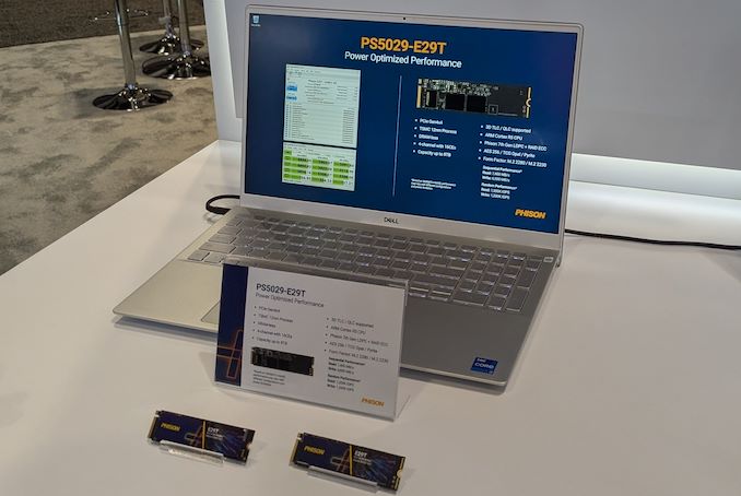
Compared to the E27T, the key update is the use of a newer LDPC engine that enables better SSD lifespan as well as compatibility with the latest QLC flash.
The company also had a U21 USB4 PSSD reference design (complete with a MagSafe-compatible casing) on display, along with the usual CrystalDiskMark benchmark results. We were given to understand that PSSDs based on the U21 controller are very close to shipping into retail.
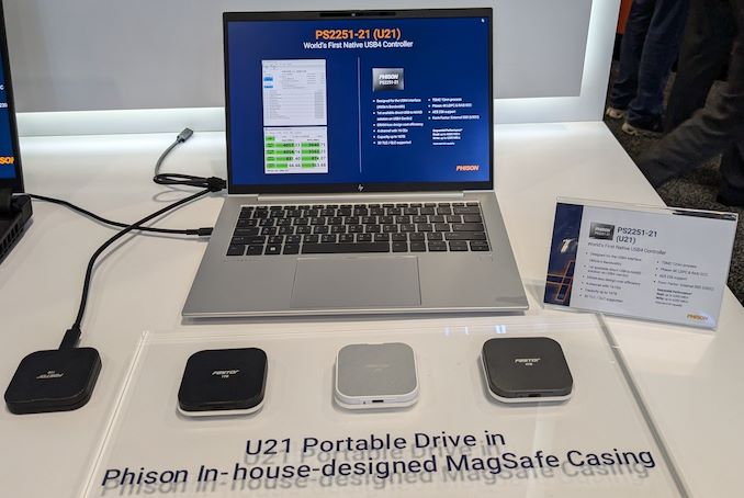
Phison has been known for taking the lead in introducing SSD controllers based on the latest and greatest interface options - be it PCIe 4.0, PCIe 5.0, or USB4. The competition is usually in the form of tier-one vendors opting for their in-house solution, or Silicon Motion stepping in a few quarters down the line after the market takes off with a more -efficient solution. With the E29T, Phison is aiming to ensure that they still have a viable play in the mainstream Gen 4 market with their latest LDPC engine and supporting the highest available NAND flash speeds.
U.S. Signs $1.5B in CHIPS Act Agreements With Amkor and SKhynix for Chip Packaging Plants
Published: Aug 9nd 2024 9:00am on AnandTech
Under the CHIPS & Science Act, the U.S. government provided tens of billions of dollars in grants and loans to the world's leading maker of chips, such as Intel, Samsung, and TSMC, which will significantly expand the country's semiconductor production industry in the coming years. However, most chips are typically tested, assembled, and packaged in Asia, which has left the American supply chain incomplete. Addressing this last gap in the government's domestic chip production plans, these past couple of weeks the U.S. government signed memorandums of understanding worth about $1.5 billion with Amkor and SK hynix to support their efforts to build chip packaging facilities in the U.S.
Amkor to Build Advanced Packaging Facility with Apple in MindAmkor plans to build a $2 billion advanced packaging facility near Peoria, Arizona, to test and assemble chips produced by TSMC at its Fab 21 near Phoenix, Arizona. The company signed a MOU that offers $400 million in direct funding and access to $200 million in loans under the CHIPS & Science Act. In addition, the company plans to take advantage of a 25% investment tax credit on eligible capital expenditures.
Set to be strategically positioned near TSMC's upcoming Fab 21 complex in Arizona, Amkor's Peoria facility will occupy 55 acres and, when fully completed, will feature over 500,000 square feet (46,451 square meters) of cleanroom space, more than twice the size of Amkor's advanced packaging site in Vietnam. Although the company has not disclosed the exact capacity or the specific technologies the facility will support, it is expected to cater to a wide range of industries, including automotive, high-performance computing, and mobile technologies. This suggests the new plant will offer diverse packaging solutions, including traditional, 2.5D, and 3D technologies.
Amkor has collaborated extensively with Apple on the vision and initial setup of the Peoria facility, as Apple is slated to be the facility's first and largest customer, marking a significant commitment from the tech giant. This partnership highlights the importance of the new facility in reinforcing the U.S. semiconductor supply chain and positioning Amkor as a key partner for companies relying on TSMC's manufacturing capabilities. The project is expected to generate around 2,000 jobs and is scheduled to begin operations in 2027.
SK hynix to Build HBM4 in the U.S.This week SK hynix also signed a preliminary agreement with the U.S. government to receive up to $450 million in direct funding and $500 million in loans to build an advanced memory packaging facility in West Lafayette, Indiana.
The proposed facility is scheduled to begin operations in 2028, which means that it will assemble HBM4 or HBM4E memory. Meanwhile, DRAM devices for high bandwidth memory (HBM) stacks will still be produced in South Korea. Nonetheless, packing finished HBM4/HBM4E in the U.S. and possibly integrating these memory modules with high-end processors is a big deal.
In addition to building its packaging plant, SK hynix plans to collaborate with Purdue University and other local research institutions to advance semiconductor technology and packaging innovations. This partnership is intended to bolster research and development in the region, positioning the facility as a hub for AI technology and skilled employment.
Intel Postpones Innovation 2024 Event, Cites Poor Finances
Published: Aug 8nd 2024 7:15am on AnandTech
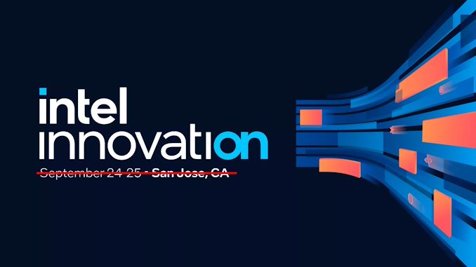
As Intel looks to streamline its business operations and get back to profitability in the face of weak revenues and other business struggles, nothing is off the table as the company looks to cut costs into 2025 – not even Intel’s trade shows. In an unexpected announcement this afternoon, Intel has begun informing attendees of its fall Innovation 2024 trade show that the event has been postponed. Previously scheduled for September of this year, Innovation is now slated to take place at some point in 2025.
Innovation is Intel’s regular technical showcase for developers, customers, and the public, and is the successor to the company’s legendary IDF show. In recent years the show has been used to deliver status updates on Intel’s fabs, introduce new client platforms like Panther Lake, launch new products, and more.
But after 3 years of shows, the future of Innovation is up in the air, as Intel has officially postponed the show – and with a less-than-assuring commitment to when it may return.
In a message posted on the Innovation 2024 website (registration required), and separately sent out via email, Intel announced the postponement of the show. In lieu of the show, Intel still plans on holding smaller developer events.
Innovation 2024 Update After careful consideration, we have made the decision to postpone our Intel-hosted event, Intel Innovation in September, until 2025. For the remainder of 2024, we will continue to host smaller, more targeted events, webinars, hackathons and meetups worldwide through Intel Connection and Intel AI Summit events, as well as have a presence at other industry moments. Depending on your development needs, please leverage the following developer resources to learn more: developer.intel.com, developer.intel.com/ai, open.intel.com and intel.com/support. Click here for a full list of Developer events. -Intel Innovation WebsiteSeparately, in a statement sent to PCMag, the company cited its current financial situation, and that they “are having to make some tough decisions as we continue to align our cost structure and look to assess how we rebuild a sustainable engine of process technology leadership.”
While Intel had not yet published a full agenda for the now-delayed show, Innovation 2024 was expected to be a major showcase for Intel’s Lunar Lake and Arrow Lake client processors, both of which are due this fall. Arrow Lake in particular is Intel’s lead product for their 20A process node – their first node implementing RibbonFETs and PowerVia backside power delivery – so its launch will be an important moment for the company. And while the postponement of Innovation won’t impact those launches, it means that Intel won’t have access to the same stage or built-in audience that comes with hosting your own trade show. Never mind the lost opportunities for software developers, who are the core audience for the show.
Officially, the show is just postponed. But given the lead time needed to reserve the San Jose Convention Center and similar venues, it’s unclear whether Intel will be able to host a show before the second half of 2025 – at which point we’d be closer to Innovation 2025, making Innovation 2024 de facto cancelled.
In the meantime, the company has already announced that they’ll be launching Lunar Lake at IFA in Germany in September. So that remains the next big trade show for Intel’s client chip group.
Microship Demonstrates Flashtec 5016 Enterprise SSD Controller
Published: Aug 8nd 2024 5:30am on AnandTech
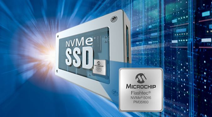
Microchip recently announced the availability of their second PCIe Gen 5 enterprise SSD controller - the Flashtec 5016. Like the 4016, this is also a 16-channel controller, but there are some key updates:
- PCIe 5.0 lane organization: Operation in x4 or dual independent x2 / x2 mode in the 5016, compared to the x8, or x4, or dual independent x4 / x2 mode in the 4016.
- DRAM support: Four ranks of DDR5-5200 in the 5016, compared to two ranks of DDR4-3200 in the 4016.
- Extended NAND support: 2400 MT/s NAND in the 4016, compared to the 3200 MT/s NAND support in the 5016.
- Performance improvements: The 5016 is capable of delivering 3.5M+ random read IOPS compared to the 3M+ of the 4016.
Microchip's enterprise SSD controllers provide a high level of flexibility to SSD vendors by providing them with significant horsepower and accelerators. The 5016 includes Cortex-A53 cores for SSD vendors to run custom applications relevant to SSD management. However, compared to the Gen4 controllers, there are two additional cores in the CPU cluster. The DRAM subsystem includes ECC support (both out-of-band and inline, as desired by the SSD vendor).
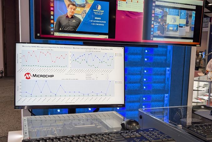
At FMS 2024, the company demonstrated an application of the neural network engines embedded in the Gen5 controllers. Controllers usually employ a 'read-retry' operation with altered read-out voltages for flash reads that do not complete successfully. Microchip implemented a machine learning approach to determine the read-out voltage based on the health history of the NAND block using the NN engines in the controller. This approach delivers tangible benefits for read latency and power consumption (thanks to lesser number of errors on the first read).
The 4016 and 5016 come with a single-chip root of trust implementation for hardware security. A secure boot process with dual-signature authentication ensures that the controller firmware is not maliciously altered in the field. The company also brought out the advantages of their controller's implementation of SR-IOV, flexible data placement, and zoned namespaces along with their 'credit engine' scheme for multi-tenant cloud workloads. These aspects were also brought out in other demonstrations.
Microchip's press release included quotes from the usual NAND vendors - Solidigm, Kioxia, and Micron. On the customer front, Longsys has been using Flashtec controllers in their enterprise offerings along with YMTC NAND. It is likely that this collaboration will continue further using the new 5016 controller.