The be quiet! Straight Power 12 750W PSU Review: Proficient Platinum Power
Published: Apr 5nd 2024 8:00am on AnandTech
In the arena of PC components, Be quiet! is a name synonymous with excellence, known for its fusion of silent functionality and exceptional performance. The company's broad range of products, from high-end power supply units (PSUs) to sophisticated cases and cooling solutions, including both air and liquid options, is crafted with a keen eye on reducing noise while maximizing efficiency. Be quiet! has earned accolades for its dedication to achieving near-silent operation across its lineup, making it a preferred choice among those in the PC enthusiast community who seek a serene computing environment. The diversity of its offerings reflects a deep understanding of the needs of tech enthusiasts and professionals alike, with each product designed to offer a blend of low noise levels and high efficiency.
Today we're looking at he Be quiet! Straight Power 12 750W PSU, a high-tier offering in Be quiet!'s PSU portfolio that exemplifies the brand's approach to product design. The Straight Power 12 series is engineered to deliver top performance and whisper-quiet operation, appealing to users who seek the optimal mix of power efficiency and sound level, without compromising on reliability and premium quality. The 750 Watt model that we are reviewing today is the weakest unit of the series, yet still enough to effortlessly power a modern gaming system with a mid-tier GPU.
SK hynix to Build $3.87 Billion Memory Packaging Fab in the U.S. for HBM4 and Beyond
Published: Apr 5nd 2024 7:00am on AnandTech
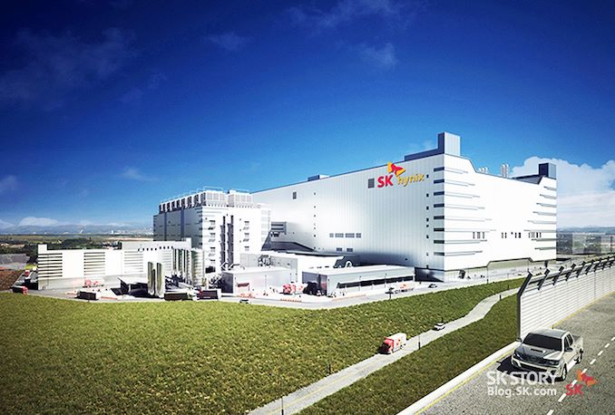
SK hynix this week announced plans to build its advanced memory packaging facility in West Lafayette, Indiana. The move can be considered as a milestone both for the memory maker and the U.S., as this is the first advanced memory packaging facility in the country and the company's first significant manufacturing operation in America. The facility will be used to build next-generation types of high-bandwidth memory (HBM) stacks when it begins operations in 2028. Also, SK hynix agreed to work on R&D projects with Purdue University.
"We are excited to become the first in the industry to build a state-of-the-art advanced packaging facility for AI products in the United States that will help strengthen supply-chain resilience and develop a local semiconductor ecosystem," said SK hynix CEO Kwak Noh-Jung.
One of The Most Advanced Chip Packaging Facility EverThe facility will handle assembly of HBM known good stacked dies (KGSDs), which consist of multiple memory devices stacked on a base die. Furthermore, it will be used to develop next-generations of HBM and will therefore house a packaging R&D line. However, the plant will not make DRAM dies themselves, and will likely source them from SK hynix's fabs in South Korea.
The plant will require SK hynix to invest $3.87 billion, which will make it one of the most advanced semiconductor packaging facilities in the world. Meanwhile, SK hynix held the investment agreement ceremony with representatives from Indiana State, Purdue University, and the U.S. government, which indicates parties financially involved in the project, but this week's event did not disclose whether SK hynix will receive any money from the U.S. government under the CHIPS Act or other funding initiatives.
The cost of the facility significantly exceeds that of packaging facilities built by other major players in the industry, such as ASE Group, Intel, and TSMC, which highlights how significant of an investment this is for SK hnix. In fact, $3.87 billion higher than advanced packaging CapEx budgets of Intel, TSMC and Samsung in 2023, based on estimates from Yole Intelligence.
Given that the fab comes online in 2028, based on SK hynix's product roadmap we'd expect that it will be used at least in part to assemble HBM4 and HBM4E stacks. Notably, since HBM4 and HBM4E stacks are set to feature a 2048-bit interface, their packaging process will be considerably more complex than the existing 1024-bit HBM3/HBM3E packaging and will require usage of more advanced tools, which is why it is poised to be more expensive than some existing advanced packaging facilities. Due to the extremely complex 2048-bit interface, many chip designers who are going to use HBM4/HBM4E are expected to integrate it directly onto their processors using hybrid bonding and not use silicon interposers. Unfortunately, it is unclear whether the SK hynix facility will be able to offer such service.
HBM is mainly used for AI and HPC applications, so it is strategically important to have its production in the U.S. Meanwhile, actual memory dies will still need to be made elsewhere, at dedicated DRAM fabs.
Purdue University CollaborationIn addition to support set to be provided by state and local governmens, SK hynix chose to establish its new facility in West Lafayette, Indiana, to collaborate with Purdue University as well as with Purdue's Birck Nanotechnology Center on R&D projects, which includes advanced packaging and heterogeneous integration.
SK hynix intends to work in partnership with Purdue University and Ivy Tech Community College to create training programs and multidisciplinary degree courses aimed at nurturing a skilled workforce and establishing a consistent stream of emerging talent for its advanced memory packaging facility and R&D operations.
"SK hynix is the global pioneer and dominant market leader in memory chips for AI," Purdue University President Mung Chiang said. "This transformational investment reflects our state and university's tremendous strength in semiconductors, hardware AI, and hard tech corridor. It is also a monumental moment for completing the supply chain of digital economy in our country through chips advanced packaging. Located at Purdue Research Park, the largest facility of its kind at a U.S. university will grow and succeed through innovation."
PCIe 7.0 Draft 0.5 Spec Available: 512 GB/s over PCIe x16 Incoming
Published: Apr 4nd 2024 8:00am on AnandTech
PCI-SIG this week released version 0.5 of the PCI-Express 7.0 specification to its members. This is the second draft of the spec and the final call for PCI-SIG members to submit their new features to the standard. The latest update on the development of the specification comes a couple months shy of a year after the PCI-SIG published the initial Draft 0.3 specificaiton, with the PCI-SIG using the latest update to reiterate that development of the new standard remains on-track for a final release in 2025.
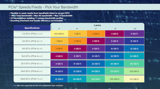
PCIe 7.0 is is the next generation interconnect technology for computers that is set to increase data transfer speeds to 128 GT/s per pin, doubling the 64 GT/s of PCIe 6.0 and quadrupling the 32 GT/s of PCIe 5.0. This would allow a 16-lane (x16) connection to support 256 GB/sec of bandwidth in each direction simultaneously, excluding encoding overhead. Such speeds will be handy for future datacenters as well as artificial intelligence and high-performance computing applications that will need even faster data transfer rates, including network data transfer rates.
To achieve its impressive data transfer rates, PCIe 7.0 doubles the bus frequency at the physical layer compared to PCIe 5.0 and 6.0. Otherwise, the standard retains pulse amplitude modulation with four level signaling (PAM4), 1b/1b FLIT mode encoding, and the forward error correction (FEC) technologies that are already used for PCIe 6.0. Otherwise, PCI-SIG says that the PCIe 7.0 speicification also focuses on enhanced channel parameters and reach as well as improved power efficiency.
Overall, the engineers behind the standard have their work cut out for them, given that PCIe 7.0 requires doubling the bus frequency at the physical layer, a major development that PCIe 6.0 sidestepped with PAM4 signaling. Nothing comes for free in regards to improving data signaling, and with PCIe 7.0, the PCI-SIG is arguably back to hard-mode development by needing to improve the physical layer once more – this time to enable it to run at around 30GHz. Though how much of this heavy lifting will be accomplished through smart signaling (and retimers) and how much will be accomplished through sheer materials improvements, such as thicker printed circuit boards (PCBs) and low-loss materials, remains to be seen.
The next major step for PCIe 7.0 is finalization of the version 0.7 of specification, which is considered the Complete Draft, where all aspects must be fully defined, and electrical specifications must be validated through test chips. After this iteration of the specification is released, no new features can be added. PCIe 6.0 eventually went through 4 major drafts – 0.3, 0.5, 0.7, and 0.9 – before finally being finalized, so PCIe 7.0 is likely on the same track.
Once finalized in 2025, it should take a few years for the first PCIe 7.0 hardware to hit the shelves. Although development work on controller IP and initial hardware is already underway, that process extends well beyond the release of the final PCIe specification.
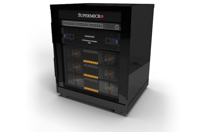
Samsung Unveils CXL Memory Module Box: Up to 16 TB at 60 GB/s
Published: Apr 3nd 2024 8:00am on AnandTech
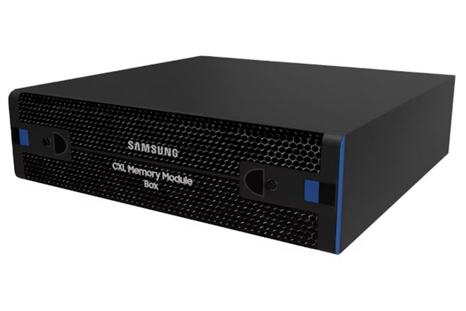
Composable disaggregated data center infrastructure promises to change the way data centers for modern workloads are built. However, to fully realize the potential of new technologies, such as CXL, the industry needs brand-new hardware. Recently, Samsung introduced its CXL Memory Module Box (CMM-B), a device that can house up to eight CXL Memory Module – DRAM (CMM-D) devices and add plenty of memory connected using a PCIe/CXL interface.
Samsung's CXL Memory Module Box (CMM-B) is the first device of this type to accommodate up to eight 2 TB E3.S CMM-D memory modules and add up to 16 TB of memory to up to three modern servers with appropriate connectors. As far as performance is concerned, the box can offer up to 60 GB/s of bandwidth (which aligns with what a PCIe 5.0 x16 interface offers) and 596 ns latency.
From a pure performance point of view, one CXL Memory Module—Box is slower than a dual-channel DDR5-4800 memory subsystem. Yet, the unit is still considerably faster than even advanced SSDs. At the same time, it provides very decent capacity, which is often just what the doctor ordered for many applications.
The Samsung CMM-B is compatible with the CXL 1.1 and CXL 2.0 protocols. It consists of a rack-scale memory bank (CMM-B), several application hosts, Samsung Cognos management console software, and a top-of-rack (ToR) switch. The device was developed in close collaboration with Supermicro, so expect this server maker to offer the product first.
Samsung's CXL Memory Module – Box is designed for applications that need a lot of memory, such as AI, data analytics, and in-memory databases, albeit not at all times. CMM-B allows the dynamic allocation of necessary memory to a system when it needs this memory and then uses DRAM with other machines. As a result, operators of datacenters can spend money on procuring expensive memory (16 TB of memory costs a lot), reduce power consumption, and add flexibility to their setups.
Gallery: Samsung Unveils CXL Memory Module Box: Up to 16 TB at 60 GB/s

Source: Samsung
Rapidus to Get $3.9 Billion in Government Aid for 2nm, Multi-Chiplet Technologies
Published: Apr 2nd 2024 1:45am on AnandTech
Rapidus, a Japan-based company developing 2nm process technology and aiming to commercialize it in 2027, will receive a huge government grant for its ongoing projects. The Japanese government will support Rapidus with subsidies totaling ¥590 billion yen ($3.89 billion). In addition to developing its 2nm production node and spending on cleanroom equipment, Rapidus will also fund the development of multi-chiplet packaging technology.
This extra funding will significantly help the company's ambitious plans. With the government's total support now at ¥920 billion ($6.068 billion), Rapidus is getting a solid push to become a significant player in the semiconductor industry. The whole project is expected to cost around ¥5 trillion ($32.983 billion), so the funding is not quite there yet. Meanwhile, the company may get enough financing with support from the Japanese government and large Japanese conglomerates like Toyota Motor and Nippon Telegraph and Telephone.
According to Atsuyoshi Koike, Rapidus's chief executive, the company is on track to start testing its production by April 2025 and aims to begin large-scale production by 2027. Commercial production of 2nm chips is set to commence sometime in 2025.
In addition to developing its 2nm fabrication process in collaboration with IBM and building its manufacturing facility, Rapidus is also working on advanced packaging technology for multi-chiplet system-in-packages (SiPs). The latest government subsidies include more than ¥50 billion ($329.85 million) for research and development in this area, the first time Japan has provided subsidies for such technologies.
It is noteworthy that Rapidus will use a section of Seiko Epson Corporation's Chitose Plant (located in Chitose City, Hokkaido) for its back-end packaging processes. This plant is near the company's fab, which is currently being built in Bibi World, an industrial park in Chitose City. This space will be dedicated to pilot-stage research and development activities.
Introspect Intros GDDR7 Test System For Fast GDDR7 GPU Design Bring Up
Published: Mar 29nd 2024 8:00am on AnandTech
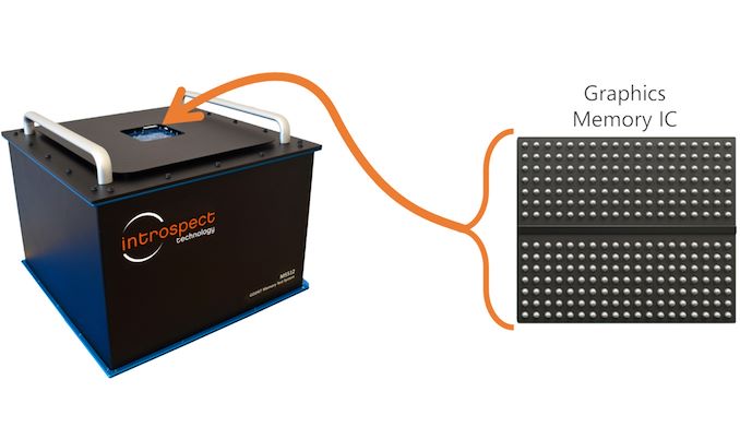
Introspect this week introduced its M5512 GDDR7 memory test system, which is designed for testing GDDR7 memory controllers, physical interface, and GDDR7 SGRAM chips. The tool will enable memory and processor manufacturers to verify that their products perform as specified by the standard.
One of the crucial phases of a processor design bring up is testing its standard interfaces, such as PCIe, DisplayPort, or GDDR is to ensure that they behave as specified both logically and electrically and achieve designated performance. Introspect's M5512 GDDR7 memory test system is designed to do just that: test new GDDR7 memory devices, troubleshoot protocol issues, assess signal integrity, and conduct comprehensive memory read/write stress tests.
The product will be quite useful for designers of GPUs/SoCs, graphics cards, PCs, network equipment and memory chips, which will speed up development of actual products that rely on GDDR7 memory. For now, GPU and SoC designers as well as memory makers use highly-custom setups consisting of many tools to characterize signal integrity as well as conduct detailed memory read/write functional stress testing, which are important things at this phase of development. But usage of a single tool greatly speeds up all the processes and gives a more comprehensive picture to specialists.
The M5512 GDDR7 Memory Test System is a desktop testing and measurement device that is equippped with 72 pins capable of functioning at up to 40 Gbps in PAM3 mode, as well as offering a virtual GDDR7 memory controller. The device features bidirectional circuitry for executing read and write operations, and every pin is equipped with an extensive range of analog characterization features, such as skew injection with femto-second resolution, voltage control with millivolt resolution, programmable jitter injection, and various eye margining features critical for AC characterization and conformance testing. Furthermore, the system integrates device power supplies with precise power sequencing and ramping controls, providing a comprehensive solution for both AC characterization and memory functional stress testing on any GDDR7 device.
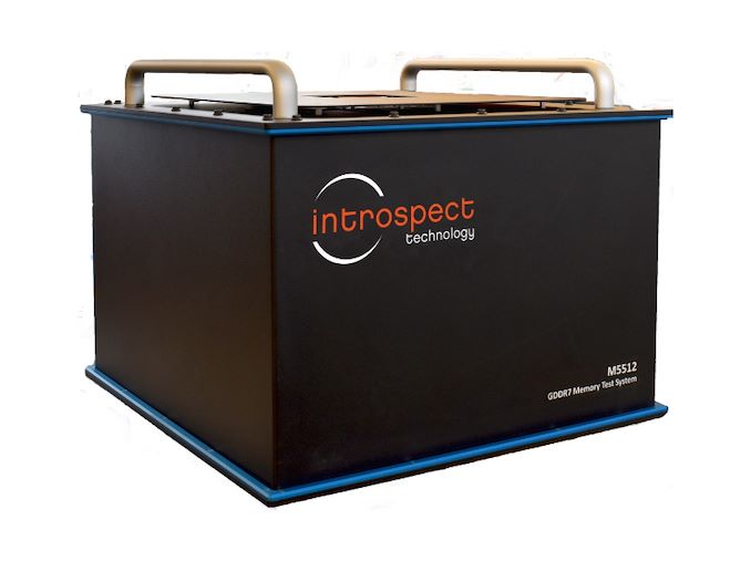
Introspects M5512 has been designed in close collaboration with JEDEC members working on the GDDR7 specification, so it promises to meet all of their requirements for compliance testing. Notably, however, the device does not eliminate need for interoperability tests and still requires companies to develop their own test algorithms, but it's still a significant tool for bootstrapping device development and getting it to the point where chips can begin interop testing.
“In its quest to support the industry on GDDR7 deployment, Introspect Technology has worked tirelessly in the last few years with JEDEC members to develop the M5512 GDDR7 Memory Test System,” said Dr. Mohamed Hafed, CEO at Introspect Technology.
Western Digital Ships 24TB Red Pro Hard Drive For NASes
Published: Mar 28nd 2024 12:00am on AnandTech
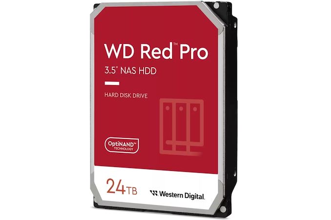
Nowadays highest-capacity hard drives are typically aimed at cloud service providers (CSPs) and enterprises, but this does not mean that creative professionals or regular users do not need them. To cater to demands of more regular consumers, Western Digital has started shipments of its Red Pro 24 TB HDDs, which are aimed at high-end NAS use for creative professionals with significant storage requirements.
Western Digital's Red Pro 24 TB hard drives come approximately 20 months after their 22 TB model hit retail in 2022, offering an incremental improvement to WD's highest-capacity NAS and consumer hard drive offering. The platform uses conventional magnetic recording (CMR), feature a 7200 RPM rotating speed, are equipped with a 512 MB cache, and use OptiNAND technology to improve reliability as well as optimize performance and power consumption. The HDDs are rated for an up to 287 MB/s media to cache transfer rate, which makes them some of the fastest hard drives around (albeit, still a bit slower compared to CSP and enterprise-oriented HDDs).
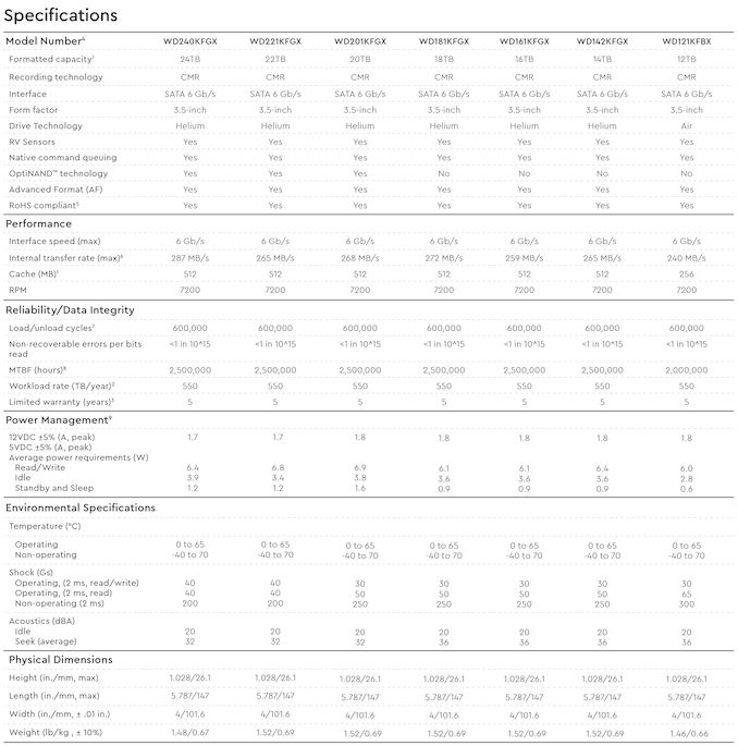
Just like other high-end network-attached storage-aimed HDDs, the Red Pro 24 TB hard drives use helium-filled platforms that are very similar to those designed for enterprise drives. Consequently, the Red Pro 24 TB HDD are equipped with rotation vibration sensors to anticipate and proactively counteract disturbances caused by increased vibration and multi-axis shock sensors to detect subtle shock events and automatically offset them with dynamic fly height technology to ensure that heads to not scratch disks.
What these drives lack compared to WD Gold and Ultraster 22 TB and 24 TB drives for enterprises and cloud datacenters is the ArmorCache feature that provides protection against power loss when write-cache is enabled (WCE mode) and enhances performance when write-cache is disabled (WCD mode).
On the reliability side of matters, Western Digital's Red Pro 24 TB HDDs are designed for 24/7 operation in vibrating environments, such as enterprise-grade NAS with loads of bays, and are rated for up to 550 TB/year workloads as well as up to 600,000 load/unload cycles, which is in line with what Western Digital's WD Gold and Ultrastar hard drives offer.
As for power consumption, the WD Red Pro 24 TB consumes up to 6.4W during read and write operations, up to 3.9W in idle mode, and up to 1.2W in standby/sleep mode.
Western Digital's Red Pro 24 TB (WD240KFGX) HDDs are now shipping to resellers as well as NAS makers, and are slated to be available shortly. Expect these hard drives to be slightly cheaper than the WD Gold 24 TB model.
The DeepCool AK620 Digital CPU Cooler Review: Big, Heavy, and Lit
Published: Mar 28nd 2024 9:00am on AnandTech
Typical CPU coolers do the job for standard heat management but often fall short when it comes to quiet operation and peak cooling effectiveness. This gap pushes enthusiasts and PC builders towards specialized aftermarket solutions designed for their unique demands. The premium aftermarket cooling niche is fiercely competitive, with brands vying to offer top-notch thermal management solutions.
Today we're shining a light on DeepCool's AK620 Digital cooler, a notable entry in the high-end CPU cooler arena. At first blush, the AK620 Digital stands out from the crowd mostly for its integrated LCD screen. Yet aesthetics aside, underneath the snappy screen is a tower cooler that was first and foremost engineered to exceed the cooling needs of the most powerful mainstream CPUs. And it's a big cooler at that: with a weight of 1.5Kg and 162mm tall, this is no lightweight heatsink and fan assembly. All of which helps to set it apart in a competitive marketplace.
HBM Revenue Poised To Cross $10B as SK hynix Predicts First Double-Digit Revenue Share
Published: Mar 28nd 2024 8:00am on AnandTech
Offering some rare insight into the scale of HBM memory sales – and on its growth in the face of unprecedented demand from AI accelerator vendors – the company recently disclosed that it expects HBM sales to make up "a double-digit percentage of its DRAM chip sales" this year. Which if it comes to pass, would represent a significant jump in sales for the high-bandwidth, high-priced memory.
As first reported by Reuters, SK hynix CEO Kwak Noh-Jung has commented that he expects HBM sales will constitute a double-digit percentage of its DRAM chip sales in 2024. This prediction corroborate with estimates from TrendForce, who believe that, industry-wide, HBM will account for 20.1% of DRAM revenue in 2024, more than doubling HBM's 8.4% revenue share in 2023.
And while SK hynix does not break down its DRAM revenue by memory type on a regular basis, a bit of extrapolation indicates that they're on track to take in billions in HBM revenue for 2024 – having likely already crossed the billion dollar mark itself in 2023. Last year, SK hynix's DRAM revenue $15.941 billion, according to Statista and TrendForce. So SK hynix only needs 12.5% of its 2024 revenues to come from HBM (assuming flat or positive revenue overall) in order to pass 2 billion in HBM sales. And even this is a low-ball estimate.
Overall, SK hynix currently commands about 50% of HBM market, having largely split the market with Samsung over the last couple of years. Given that share, and that DRAM industry revenue is expected to increase to $84.150 billion in 2024, SK hynix could earn as much as $8.45 billion on HBM in 2024 if TrendForce's estimates prove accurate.
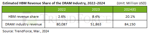
It should be noted that with demand for AI servers at record levels, all three leading makers of DRAM are poised to increase their HBM production capacity this year. Most notable here is a nearly-absent Micron, who was the first vendor to start shipping HBM3E memory to NVIDIA earlier this year. So SK hynix's near-majority of the HBM market may falter some this year, though with a growing pie they'll have little reason to complain. Ultimately, if sales of HBM reach $16.9 billion as projected, then all memory makers will be enjoying significant HBM revenue growth in the coming months.
Sources: Reuters, TrendForce
GDDR7 Approaches: Samsung Lists GDDR7 Memory Chips on Its Product Catalog
Published: Mar 27nd 2024 3:00am on AnandTech
Now that JEDEC has published specification of GDDR7 memory, memory manufacturers are beginning to announce their initial products. The first out of the gate for this generation is Samsung, which has has quietly added its GDDR7 products to its official product catalog.
For now, Samsung lists two GDDR7 devices on its website: 16 Gbit chips rated for an up to 28 GT/s data transfer rate and a faster version running at up to 32 GT/s data transfer rate (which is in line with initial parts that Samsung announced in mid-2023). The chips feature a 512M x32 organization and come in a 266-pin FBGA packaging. The chips are already sampling, so Samsung's customers – GPU vendors, AI inference vendors, network product vendors, and the like – should already have GDDR7 chips in their labs.
The GDDR7 specification promises the maximum per-chip capacity of 64 Gbit (8 GB) and data transfer rates of 48 GT/s. Meanwhile, first generation GDDR7 chips (as announced so far) will feature a rather moderate capacity of 16 Gbit (2 GB) and a data transfer rate of up to 32 GT/s.

Performance-wise, the first generation of GDDR7 should provide a significant improvement in memory bandwidth over GDDR6 and GDDR6X. However capacity/density improvements will not come until memory manufacturers move to their next generation EUV-based process nodes. As a result, the first GDDR7-based graphics cards are unlikely to sport any memory capacity improvements. Though looking a bit farther down the road, Samsung and SK Hynix have previously told Tom's Hardware that they intend to reach mass production of 24 Gbit GDDR7 chips in 2025.
Otherwise, it is noteworthy that SK Hynix also demonstrated its GDDR7 chips at NVIDIA's GTC last week. So Samsung's competition should be close behind in delivering samples, and eventually mass production memory.
Source: Samsung (via @harukaze5719)