Western Digital Previews 4 TB SD Card: World's Highest-Capacity
Published: Apr 11nd 2024 6:30am on AnandTech

Western Digital this week is previewing the industry's first 4 TB SD card. The device is being showcased at the NAB trade show for broadcasters and content creators and will be released commercially in 2025.
Western Digital's SanDisk Extreme Pro SDUC 4 TB SD card complies with the Secure Digital Ultra Capacity standard (SDUC, which enables up to 128TB). The card uses the Ultra High Speed-I (UHS-I) interface and is rated for speed Class 10, therefore supporting a minimum speed of 10 MB/s and a maximum data transfer rate of 104 MB/s when working in UHS104 (SDR104) mode (there is a catch about performance, but more on that later). WD's SD card is also rated to meet Video Speed Class V30, supporting a minimal sequential write speed of 30 MB/s, which is believed to be good enough for 8K video recording, above and beyond the 4K video market that Western Digital is primarily aiming the forthcoming card at.
For now, Western Digital is not disclosing what NAND is in the SanDisk Extreme Pro SDUC 4 TB SD card. Given the high capacity and relatively distant 2025 release date, WD may be targetting this as one of their first products to use their forthcoming BiCS 9 NAND.
And while not listed in WD's official press release, we would be surprised if the forthcoming card didn't also support the off-spec DDR200/DDR208 mode, which allows for higher transfer rates than the UHS-I standard normally allows via double data rate signaling. Western Digital's current-generation SanDisk Extreme Pro SDXC 1 TB SD card already supports that mode, allowing it to reach read speeds as high as 170 MB/s, so it would be surprising to see the company drop it from newer products. That said, the catch with DDR208 remains the same as always: it's a proprietary mode that requires a compatible host to make use of.
Western Digital has not disclosed how much will its SanDisk Extreme Pro SDUC 4 TB SD card cost. A 1 TB SanDisk Extreme Pro card costs $140, so one can make guesses about the price of a 4 TB SD card that uses cutting-edge NAND.
AMD Quietly Launches Ryzen 7 8700F and Ryzen 5 8400F Processors
Published: Apr 11nd 2024 3:30am on AnandTech
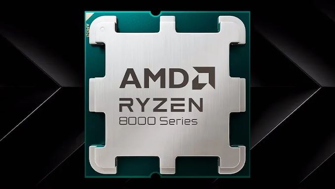
AMD has recently expanded its Ryzen 8000 series by introducing the Ryzen 7 8700F and Ryzen 5 8400F processors. Initially launched in China, these chips were added to AMD's global website, signaling they are available worldwide, apparently from April 1st. Built from the recent Zen 4-based Phoenix APUs using the TSMC 4nm node as their Zen 4 mobile chips, these new CPUs lack integrated graphics. However, the Ryzen 7 8700F does include the integrated Ryzen AI NPU for added capabilities in a world currently dominated by AI and moving it directly into the PC.
The company's decision to announce these chips in China aligns with its strategy to offer Ryzen solutions at every price point in the market. Although AMD didn't initially disclose the full specifications of these F-series models, and we did reach out to the company to ask about them, they refused to discuss them with us. Their listing on the website has now been updated with a complete list of specifications and features, with everything but the price mentioned.
AMD Ryzen 8000G vs. Ryzen 8000F Series (Desktop) Zen 4 (Phoenix) AnandTech Cores/Threads Base Freq Turbo Freq GPU GPU Freq Ryzen AI (NPU) L3 Cache (MB) TDP MSRP Ryzen 7 Ryzen 7 8700G 8/16 4200 5100 R780M 12 CUs 2900 Y 16 65W $329 Ryzen 7 8700F 8/16 4100 5000 - - Y 16 65W ? Ryzen 5 Ryzen 5 8600G 6/12 4300 5000 R760M 8 CUs 2800 Y 16 65W $229 Ryzen 5 8400F 6/12 4200 4700 - - N 16 65W ?The Ryzen 7 8700F features an 8C/16T design, with 16MB of L3 cache and the same 65W TDP as the Ryzen 7 8700G. Although the base clock speed is 4.1 GHz, it boosts to 5.0 GHz; this is 100 MHz less on both base/boost clocks than the 8700G. Meanwhile, the Ryzen 5 8400F is a slightly scaled-down version of the Ryzen 8600G APU, with 6C/12, 16MB of L3 cache, and again has a 100 MHz reduction to base clocks compared to the 8600G. Unlike the Ryzen 5 8400F, the Ryzen 7 8700F keeps AMD's Ryzen AI NPU, adding additional capability for generative AI.
The Ryzen 5 8400F can boost up to 4.7 GHz, 300 MHz slower than the Ryzen 5 8600G. AMD also allows overclocking for these new F-series chips, which means users could potentially boost the performance of these processors to match their G-series equivalents.
Pricing details are still pending, but to remain competitive, AMD will likely need to price these CPUs below the 8700G and 8600G, as well as the Ryzen 7 7700 and Ryzen 5 7600. These CPUs offer, albeit very limited, integrated graphics and have double the L3 cache capacity, along with higher boost clocks than the 8000F series chips, so pricing is something to consider whenever pricing becomes available.
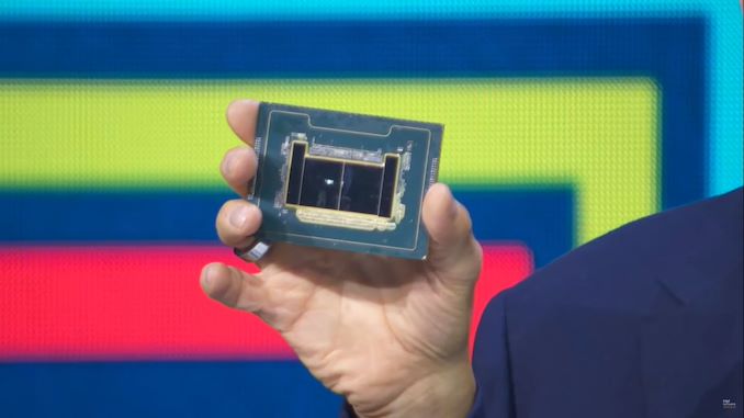
Intel Teases Lunar Lake At Intel Vision 2024: 100+ TOPS Overall, 45 TOPS From NPU Alone
Published: Apr 11nd 2024 1:00am on AnandTech
During the main keynote at Intel Vision 2024, Intel CEO Pat Gelsinger flashed a completed Lunar Lake chip off, much like EVP and General Manager of Intel's Client Computing Group (CCG) Michelle Johnston Holthaus did back at CES 2024. The contrast between the two glimpses of the Lunar Lake chip is that Pat Gelsinger gave us something juicier than just a photo op. He clarified and claimed the levels of AI performance we can expect to see when Lunar Lake launches.
According to Intel's CEO Pat Gelsinger, Lunar Lake, scheduled to be launched towards the end of this year, is set to raise the bar even further regarding on-chip AI capabilities and performance. At Intel's own Vision event, aptly named Intel Vision, current CEO of Intel Pat Gelsinger stated during his presentation that Lunar Lake will be the 'flagship SoC' for the next generation of AI PCs. Intel claims that Lunar Lake will have 3X the AI performance of their current Meteor Lake SoC, which is impressive as Meteor Lake is estimated to be running around 34 TOPS combined with the NPU, GPU, and CPU.
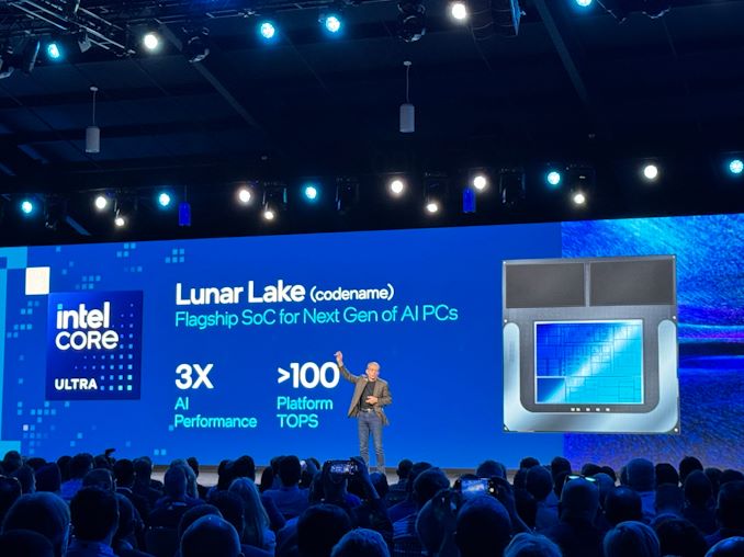
Factoring in the NPU within Meteor Lake, 11 of the 34 TOPS come solely from the NPU. Still, Intel claims that the NPU on Lunar Lake will hit a large 45 TOPs, akin to the Hailo-10 add-in card and similar to Qualcomm's Snapdragon X Elite processor. Factoring in the integrated graphics and the compute cores, Intel is claiming a combined total of over 100 TOPS, and with Microsoft's self-imposed guidelines of what constitutes an 'AI PC' coming in at 40 TOPS, Intel's NPU fits the bill.
Intel also alludes to how they are gaining a load of TOPS performance from the NPU, whether that be with new technologies; the NPU will likely be built in a more advanced node, perhaps Intel 18A. Another thing Intel didn't highlight was how they were measuring the TOPS performance, whether that be INT8 or INT4.
Still, one thing is clear: Intel wants to increase on-chip AI capabilities in desktop PCs and notebooks with each generation. Intel is also attempting to leverage more AI performance to help boost its goal to ship 100 million AI PCs by the end of 2025. Intel has already announced that it's shipped 5 million thus far and plans to sell another 40 million units by the end of the year.
The Intel Core Ultra 7 155H Review: Meteor Lake Marks A Fresh Start To Mobile CPUs
Published: Apr 11nd 2024 8:30am on AnandTech
One of the most significant talking points of the last six months in mobile computing has been Intel and their disaggregated Meteor Lake SoC architecture. Meteor Lake, along with the new Core and Core Ultra naming scheme, also heralds the dawn of their first tiled architecture for the mobile landscape on the latest Intel 4 node with Foveros packaging. In December last year, Intel unveiled their premier Meteor lake-based Core Ultra H series, with five SKUs ranging from two with 4P+8E+2LP/18T and three with 6P+8E+2LP/22T models. Since then, many vendors and manufacturers have launched notebooks capitalizing on Intel's latest multi-tiled Meteor Lake SoC architecture as the heart of power and performance, driving their latest models into 2024.
Today, we will focus on an attractive ultrabook via the ASUS Zenbook 14 OLED (UX3405MA), which features a thin and light design and is powered by Intel's latest Meteor Lake Core Ultra 7 155H processor. While much of the attention is going to come on how the Intel Core Ultra 7 155H with its 6P+8E+2LP/22T configuration and 8 Arc Xe integrated graphics cores will perform, the ASUS Zenbook 14 OLED UX3405MA has plenty of features within its sleek Ponder Blue colored shell to make it very interesting. Included is a 14" 3K (2880 x 1800) touchscreen OLED panel with a 120 Hz refresh rate, 32 GB of LPDDR5X memory (soldered), and a 1 TB NVMe M.2 SSD for storage.
Intel To Discontinue Boxed 13th Gen Core CPUs for Enthusiasts
Published: Apr 10nd 2024 8:00am on AnandTech
In an unexpected move, Intel has announced plans to phase out the boxed versions of its enthusiasts-class 13th Generation Core 'Raptor Lake' processors. According to a product change notification (PCN) published by the company last month, Intel plans to stop shipping these desktop CPUs by late June. In its place will remain Intel's existing lineup of boxed 14th Generation Core processors, which are based on the same 'Raptor Lake' silicon and typically carry higher performance for similar prices.
Intel customers and distributors interested in getting boxed versions 13th Generation Core i5-13600K/KF, Core i7-13700K/KF, and Core i9-13900K/KF/KS 'Raptor Lake' processors with unlocked multiplier should place their orders by May 24, 2024. The company will ship these units by June 28, 2024. Meanwhile, the PCN does not mention any change to the availability of tray versions of these CPUs, which are sold to OEMs and wholesalers.
The impending discontinuation of Intel's boxed 13th Generation Core processors comes as the company's current 14th Generation product line, 'Raptor Lake Refresh' is largely a rehash of the same silicon at slightly higher clockspeeds. Case in point: all of the discontinued SKUs are based on Intel's B0 Raptor Lake silicon, which is still being used for their 14th Gen counterparts. So Intel has not discontinued producing any Raptor Lake silicon; only the number of retail SKUs is getting cut-down.
As outlined in our 14th Generation Core/Raptor Lake Refresh review, the 14th Gen chips largely make their 13th Gen counterparts redundant, offering better performance at every tier for the same list price. And with virtually all current generation motherboards supporting both generation of chips, apparently Intel feels there's little reason to keep around what's essentially older, slower SKUs of the same silicon.
Interestingly, the retirement of the enthusiast-class 13th Generation Core chips is coming before Intel discontinues their even older 12th Generation Core 'Alder Lake' processors. 12th Gen chips are still available to this day in both boxed and tray versions, and the Alder Lake silicon itself is still widely in use in multiple product families. So even though Alder Lake shares the same platform as Raptor Lake, the chips based on that silicon haven't been rendered redundant in the same way that 13th Gen Core chips have.
Ultimately, it would seem that Intel is intent on consolidating and simplifying its boxed retail chip offerings by retiring their near-duplicate SKUs. Which for PC buyers could present a minor opportunity for a deal, as retailers work to sell off their remaining 13th Gen enthusiast chips.
Report: Impact of Taiwanese Earthquake on DRAM Output to be Negligible in Q2
Published: Apr 10nd 2024 6:00am on AnandTech
Following the magnitude 7.2 earthquake that struck Taiwan on April 3, 2024, there was immediate concern over what impact this could have on chip production within the country. Even for a well-prepared country like Taiwan, the tremor was the strongest quake to hit the region in 25 years, making it no small matter. But, according to research compiled by TrendForce, the impact on the production of DRAM will not be significant. The market tracking company believes that Taiwanese DRAM industry has remained largely unaffected, primarily due to their robust earthquake preparedness measures.
There are four memory makers in Taiwan: Micron, the sole member of the "big three" memory manufacturers on the island, runs two fabs. Meanwhile among the smaller players is Nanya (which has one fab), Winbond (which makes specialty memory at one fab), and PSMC (which produces specialty memory at one plant). The study found that these DRAM producers quickly resumed full operations, but had to throw away some wafers. The earthquake is estimated to have a minor effect on Q2 DRAM production, with a negligible 1% impact, TrendForce claims
In fact, as Micron is ramping up production of DRAM on its 1alpha and 1beta nm process technologies, it increases bit production of memory, which will positively affect supply of commodity DRAM in Q2 2025.

Following the earthquake, there was a temporary halt in quotations for both the contract and spot DRAM markets. However, the spot market quotations have already largely resumed, while contract prices have not fully restarted. Notably, Micron and Samsung ceased issuing quotes for mobile DRAM immediately after the earthquake, with no updates provided as of April 8th. In contrast, SK hynix resumed quotations for smartphone customers on the day of the earthquake and proposed more moderate price adjustments for Q2 mobile DRAM.
TrendForce anticipates a seasonal contract price increase for Q2 mobile DRAM of between 3% and 8%. This moderate increase is partly due to SK hynix's more restrained pricing strategy, which is likely to influence overall pricing strategies across the industry. The earthquake's impact on server DRAM primarily affected Micron's advanced fabrication nodes, potentially leading to a rise in final sale prices for Micron's server DRAM, according to TrendForce. However, the exact direction of future prices remains to be seen.
Meanwhile, DRAM fabs outside of Taiwan have none been directly affected by the quake. This includes Micron's HBM production line in Hiroshima, Japan, and Samsung's and SK hynix's HBM lines in South Korea, all of which are apparently operating with business as usual.
In general, the DRAM industry has shown resilience in the face of the earthquake, with minimal disruptions and a quick recovery. The abundant inventory levels for DDR4 and DDR5, coupled with weak demand, suggest that any slight price elevations caused by the earthquake are expected to normalize quickly. The only potential outlier here is DDR3, which is nearing the end of its commercial lifetime and production is already decreasing.
Google Develops In-House Arm 'Axion' CPU for Datacenters
Published: Apr 9nd 2024 6:00am on AnandTech
Google was among the first hyperscalers build custom silicon for its services, starting first with tensor processing units (TPUs) for its AI initiatives, and then video transcoding units (VCUs) for the YouTube service. But unlike its industry peers, the company has been slower to adopt custom CPU designs, prefering to stick to off-the-shelf chips from the major CPUs. This is finally changing at Google, with the announcement that the company has developed its own in-house datacenter CPU, the Axion.
Google's Axion processor is based on the Arm Neoverse V2 (Arm v9) platform, which is Arm's current-generation design for high-performance server CPUs, and is already employed in other chips such as NVIDIA's Grace. Within Google, Axion is aimed at a wide variety of workloads, including web and app servers, data analytics, microservices, and AI training. Google claims that the Axion processors boast up to 50% higher performance and up to 60% better energy efficiency compared to current-generation x86-based processors, as well as offer a 30% higher performance compared to competing Arm-based CPUs for datacenters. Though as is increasingly common for the cryptic cloud side of Google's business, least for now the company isn't specifying what processors they're comparing Axion to in these metrics.
While Google is not disclosing core counts or the full specifications of its Axion CPUs, the company is revealing that they are incorporating their own secret sauce into the silicon in the form of the company's Titanium purpose-built microcontrollers. These microcontrollers are designed to handle basic operations like networking and security, as well as offload storage I/O processing to Hyperdisk block storage service. As a result of this offloading, virtually all of the CPU core resources should be available to actual workloads. As for the chip's memory subsystem, Axion uses conventional dual-rank DDR5 memory modules.
"Google's announcement of the new Axion CPU marks a significant milestone in delivering custom silicon that is optimized for Google's infrastructure, and built on our high-performance Arm Neoverse V2 platform," said Rene Haas, CEO of Arm. "Decades of ecosystem investment, combined with Google's ongoing innovation and open-source software contributions ensure the best experience for the workloads that matter most to customers running on Arm everywhere."
Google has deployed its new processors for its own services, including BigTable, Spanner, BigQuery, and YouTube Ads and is ready to offer instances based on these Arm CPUs to its customers that can use software developed for Arm.
Sources: Google, Wall Street Journal
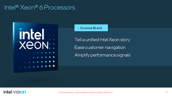
Intel Unveils New Branding For 6th Generation Xeon Processors: Intel Xeon 6
Published: Apr 9nd 2024 11:35am on AnandTech
At Intel's Vision 2024 event, which is held in Phoenix, AZ, has seen several key announcements. Still, perhaps one that has flown under the radar is their 6th Generation Xeon platform built on their Intel 3 node, which is aptly named Intel Xeon 6. It is set to launch in the future with two primary variants, including a Performance (P) core family based on Intel's Sierra Forest architecture and an Efficiency (E) core-flavored variant based on Granite Rapids. Intel's current branding surrounds a number of key nomenclatures, including Xeon 'Scalable,' which is used on the current 5th Generation Xeon Scalable Platform (Emerald Rapids).
As part of Intel's Enterprise AI ecosystem, and set to launch sometime in the second half of 2024, the Intel Xeon 6 (Granite Rapids), Intel is 'evolving' the naming structure and branding for their Xeon line-up by ditching the 'scalable' from the nomenclature and opting to stick with the generation number.
Over the last year, we've extensively covered Intel's Granite Rapids and Sierra Forest. For more information about Granite Rapids and Sierra Forest, here are some of our key pieces:
- Hot Chips 2023: Intel Details More on Granite Rapids and Sierra Forest Xeons
- Intel Previews Sierra Forest with 288 E-Cores, Announces Granite Rapids-D for 2025 Launch at MWC 2024
- IFS Reborn as Intel Foundry: Expanded Foundry Business Adds 14A Process To Roadmap
Intel debuted their Xeon Scalable branded processors in 2017 with the launch of the Xeon Platinum 8100 series, which was built using their Skylake microarchitecture. Moving forward to 2024, Intel is looking to build an ecosystem befitting the current demands of technologies within key areas such as data centers, Edge, and the PC. Intel is laying the foundations for what it calls 'Intel Enterprise AI.' Using a vast array of frameworks and accelerators and working closely with partners, ISVs, and GSIs to create a large and open ecosystem, the newly branded Intel Xeon 6 platforms will be key in the enterprise market as we advance.
Intel has adopted a newer and simpler nomenclature for Granite Rapids and Sierra Forest, starting with the Intel Xeon 6 processors. Intel's Sierra Forest Xeon 6 processors are set to launch in Q2 of 2024, which include a chip featuring 288 E-cores. It will be the first generation to adopt this new branding, which is designed to ease customer navigation between models. Note that the Performance (P) core Intel Xeon 6 processors built on Granite Rapids will come later.
However, the key parts include the Xeon naming for enterprise, workstation, server, and data center, which isn't changing. The second part is the generation number, which is highlighted in the 6 marking it as the 6th Generation of Intel's Xeon platform.
As mentioned, Intel's Xeon 6 processors, based on their Sierra Forest architecture, are set to launch in Q2 2024, while the Granite Rapids Xeon 6 platform is expected to come sometime in the second half of 2024.
Gallery: Intel Vision 2024 Press Deck


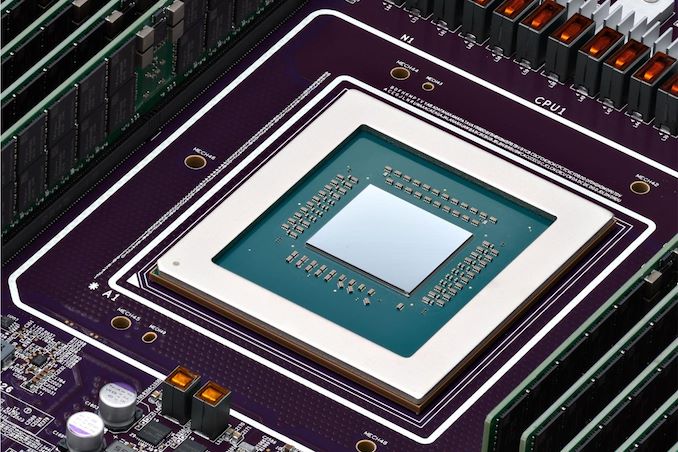
Intel Introduces Gaudi 3 AI Accelerator: Going Bigger and Aiming Higher In AI Market
Published: Apr 9nd 2024 11:35am on AnandTech
Intel this morning is kicking off the second day of their Vision 2024 conference, the company’s annual closed-door business and customer-focused get-together. While Vision is not typically a hotbed for new silicon announcements from Intel – that’s more of an Innovation thing in the fall – attendees of this year’s show are not coming away empty handed. With a heavy focus on AI going on across the industry, Intel is using this year’s event to formally introduce the Gaudi 3 accelerator, the next-generation of Gaudi high-performance AI accelerators from Intel’s Habana Labs subsidiary.
The latest iteration of Gaudi will be launching in the third quarter of 2024, and Intel is already shipping samples to customers now. The hardware itself is something of a mixed bag in some respects (more on that in a second), but with 1835 TFLOPS of FP8 compute throughput, Intel believes it’s going to be more than enough to carve off a piece of the expansive (and expensive) AI market for themselves. Based on their internal benchmarks, the company expects to be able beat NVIDIA’s flagship Hx00 Hopper architecture accelerators in at least some critical large language models, which will open the door to Intel grabbing a larger piece of the AI accelerator market at a critical time in the industry, and a moment when there simply isn’t enough NVIDIA hardware to go around.
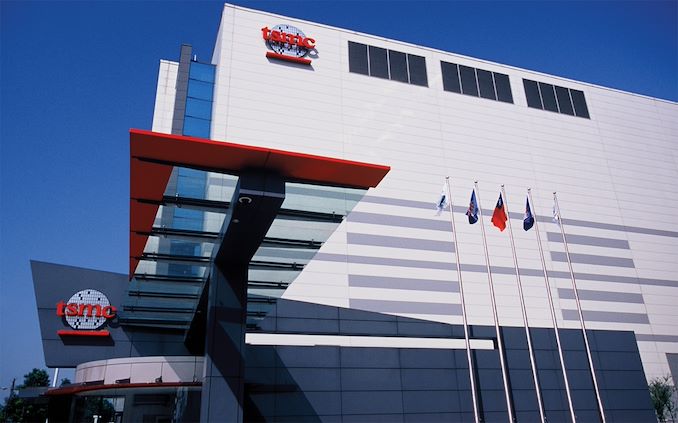
TSMC to Receive $6.6B Under US CHIPS Act, Set to Build 2nm Fab in Arizona
Published: Apr 8nd 2024 4:30am on AnandTech
TSMC has entered into a preliminary agreement with the U.S. Department of Commerce, securing up to $6.6 billion in direct funding and access to up to $5 billion in loans under the CHIPS and Science Act. With this latest round of support from the U.S. government, TSMC in turn will be adding a third fab to their Arizona project, with its investment in the region soaring to more than $65 billion. This move not only signifies the largest foreign direct investment in Arizona but also marks one of the biggest support packages that the U.S. government plans to make under the CHIPS Act, second only to Intel's $8.5 billion award last month.
TSMC is currently equipping its Fab 21 phase 1 and expects that it will start making chips using N4 and N5 (4 nm and 5 nm-class) process technologies in the first half of 2025. TSMC's Fab 21 phase 2 will commence operations in 2028, and will make chips on N3 and N2 (3 nm and 2 nm-class) production nodes. The newly-announced third fab (designation TBD) is set to manufacture chips on processes of 2 nm-class or beyond, with the start of production anticipated by the end of the decade.
TSMC has not announced a planned capacity for the new fab, only noting that it will be similar to the other two Arizona fabs, boasting a cleanroom space roughly twice as large as that of a typical "industry-standard logic fab." If it is sized similarly to the other Arizona fabs, then this strongly implies that the new fab will be another MegaFab-class facility – a mid-range fab producing around 25,000 wafer starts per month. TSMC does operate even larger fabs – the 100K WSPM GigaFab – though to date they've yet to build any of these outside of Taiwan.
“The CHIPS and Science Act provides TSMC the opportunity to make this unprecedented investment and to offer our foundry service of the most advanced manufacturing technologies in the United States,” said TSMC Chairman Dr. Mark Liu. “Our U.S. operations allow us to better support our U.S. customers, which include several of the world’s leading technology companies. Our U.S. operations will also expand our capability to trailblaze future advancements in semiconductor technology.”
The construction of three fabs in Arizona is poised to generate approximately 6,000 direct high-tech jobs, contributing significantly to the creation of a skilled workforce. This workforce is expected to play a crucial role in fostering a dynamic and competitive global semiconductor ecosystem. Moreover, the project is projected to create over 20,000 construction jobs, in addition to spawning tens of thousands of indirect jobs related to suppliers and consumer services.
AMD, Apple, and NVIDIA fully support TSMC's project and all of them expressed interest in using TSMC's capacities in the U.S.
“Today’s announcement highlights the strong commitment from Secretary Raimondo and the entire administration to ensure the U.S. plays a central role creating a more geographically diverse and resilient semiconductor supply chain,” said AMD Chair and CEO Lisa Su. “TSMC has a long track record of providing the leading-edge manufacturing capabilities that have enabled AMD to focus on what we do best, designing high-performance chips that change the world. We are committed to our partnership with TSMC and look forward to building our most advanced chips in U.S.”
TSMC's ventures in Arizona have encountered obstacles, such as setbacks caused by labor shortages and doubts about the U.S. governmental funding. As a result, production at the second facility has been postponed from 2026 to 2028. Moreover, Bloomberg has reported that at least one supplier for TSMC has called off its intended project in Arizona, attributing the decision to challenges in securing a workforce. The address the workforce issues, the TSMC grant includes a $50 million allocation for training of the local workforce.