Report: SK Hynix Mulls Building $4 Billion Advanced Packaging Facility in Indiana
Published: Mar 26nd 2024 7:00am on AnandTech
SK hynix is considering whether to build an advanced packaging facility in Indiana, reports the Wall Street Journal. If the company proceeds with the plan, it intends to invest $4 billion in it and construct one of the world's largest advanced packaging facilities. But to accomplish the project, SK hynix expects it will need help from the U.S. government.
Acknowledging the report but stopping short of confirming the company's plans, a company spokeswoman told the WSJ that SK hynix "is reviewing its advanced chip packaging investment in the U.S., but hasn’t made a final decision yet."
Companies like TSMC and Intel spend billions on advanced packaging facilities, but so far, no company has announced a chip packaging plant worth quite as much as SH hynix's $4 billion. The field of advanced packaging – CoWoS, passive silicon interposers, redistribution layers, die-to-die bonding, and other cutting edge technologies – has seen an explosion in demand in the last half-decade. As bandwidth advances with traditional organic packaging are largely played out, chip designers have needed to turn to more complex (and difficult to assemble) technologies in order to wire up an ever larger number of signals at ever-higher transfer rates. Which has turned advanced packaging into a bottleneck for high-end chip and accelerator production, driving a need for additional packaging facilities.
If SK hynix approves the project, the advanced packaging facility is expected to begin operations in 2028 and could create as many as 1,000 jobs. With an estimated cost of $4 billion, the plant is poised to become one of the largest advanced packaging facilities in the world.
Meanwhile, government backing is thought to be essential for investments of this scale, with potential state and federal tax incentives, according to the report. These incentives form part of a broader initiative to bolster the U.S. semiconductor industry and decrease dependence on memory produced in South Korea.
SK hynix is the world's leading producer of HBM memory, and is one of the key HBM suppliers to NVIDIA. Next generations of HBM memory (including HBM4 and HBM4E) will require even closer collaboration between chip designers, chipmakers, and memory makers. Therefore, packaging HBM in America could be a significant benefit for NVIDIA, AMD, and other U.S. chipmakers.
Investing in the Indiana facility will be a strategic move by SK hynix to enhance its advanced chip packaging capabilities in general and demonstrating dedication to the U.S. semiconductor industry.
Intel Announces Expansion to AI PC Dev Program, Aims to Reach More Software & Hardware Devs
Published: Mar 26nd 2024 6:00am on AnandTech

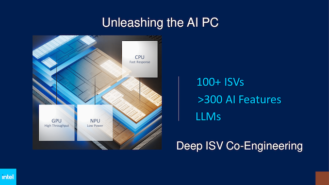
Today, Intel announced that it is looking to progress its AI PC Acceleration program further by offering various new toolkits and devkits designed for software and hardware AI developers under a new AI PC Developer Program sub-initiative. Originally launched on October 23, the AI PC Acceleration program was created to connect hardware vendors with software developers, using Intel's vast resources and experience to develop a broader ecosystem as the world pivots to one driven by AI development.
Intel aims to maximize the potential of AI applications and software and broaden the whole AI-focused PC ecosystem by aiming for AI within 100 million Intel-driven AI PCs by 2025. The AI PC Developer Program aims to simplify the adoption of new AI technologies and frameworks on a larger scale. It provides access to various tools, workflows, AI-deployment frameworks, and developer kits, allowing developers to take advantage of the latest NPU found within Intel's Meteor Lake Core Ultra series of processors.
It also offers centralized resources like toolkits, documentation, and training to allow developers to fully utilize their software and hardware in tandem with the technologies associated with Meteor Lake (and beyond) to enhance AI and machine learning application performance. Such toolkits are already broadly used by developers, including Intel's open-source OpenVino.
Furthermore, this centralized resource platform is designed to streamline the AI development process, making it more efficient and effective for developers to integrate AI capabilities into their applications. It is designed to play a crucial role in Intel’s strategy to not only advance AI technology but also to make it more user-friendly and adaptable to various real-world applications.

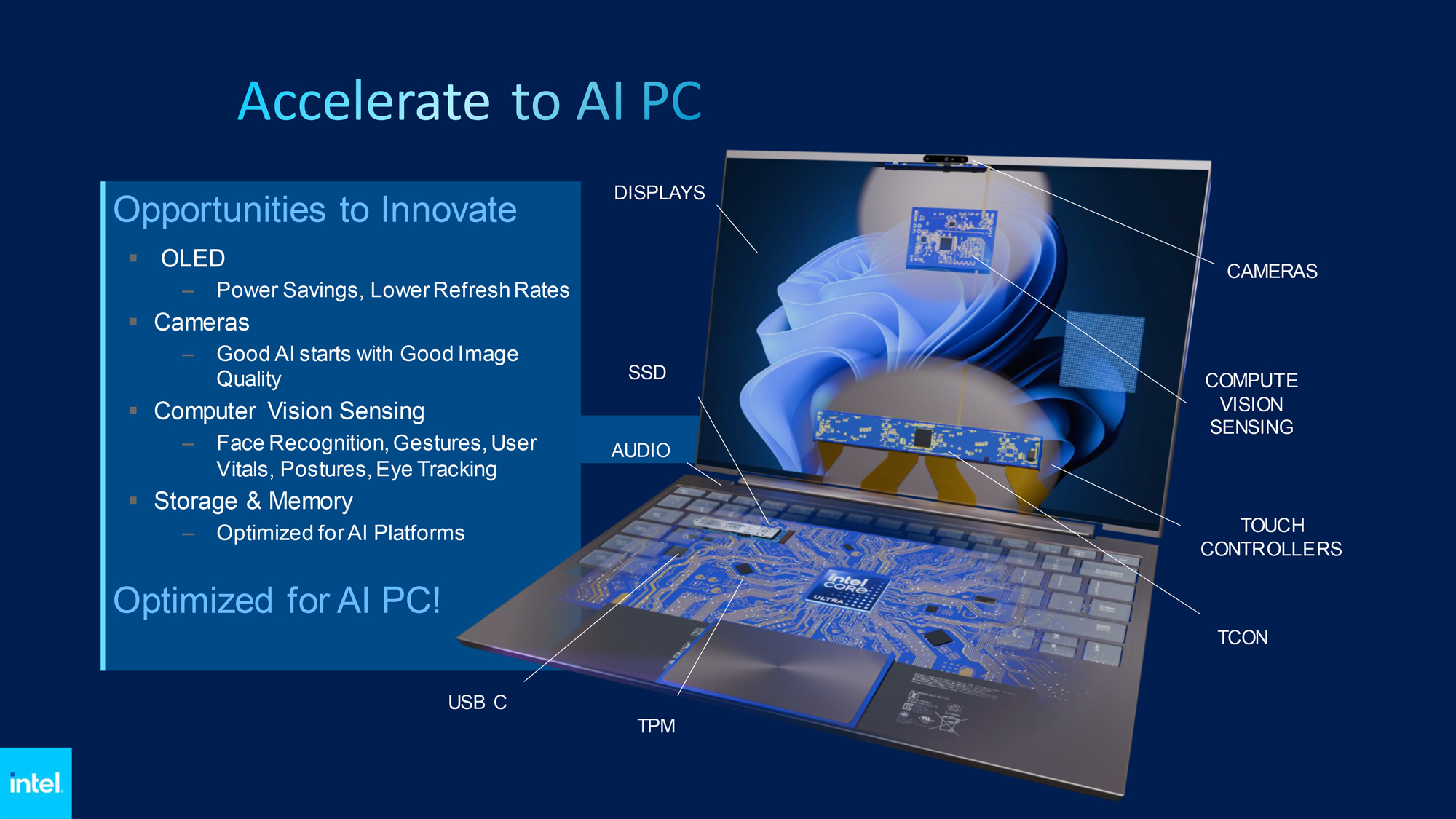
Notably, this is both a software and a hardware play. Intel isn't just looking to court more software developers to utilize their AI resources, but they also want to get independent hardware vendors (IHVs) on board. OEMs and system assemblers are largely already covered under Microsoft's requirements for Windows certification, but Intel wants to get the individual parts vendors involved as well. How can AI be used to improve audio performance? Display performance? Storage performance? That's something that Intel wants to find out.
"We have made great strides with our AI PC Acceleration Program by working with the ecosystem. Today, with the addition of the AI PC Developer Program, we are expanding our reach to go beyond large ISVs and engage with small and medium sized players and aspiring developers" said Carla Rodriguez, Vice President and General Manager of Client Software Ecosystem Enabling. "Our goal is to drive a frictionless experience by offering a broad set of tools including the new AI-ready Developer Kit,"
The Intel AI PC Acceleration Program offers 24/7 access to resources and early reference hardware so that both ISVs and software developers can create and optimize workloads before launching retail components. Developers can join the AI PC Acceleration Program at their official webpage or email [email protected] for further information


Report: China to Pivot from AMD & Intel CPUs To Domestic Chips in Government PCs
Published: Mar 26nd 2024 4:00am on AnandTech
China has initiated a policy shift to eliminate American processors from government computers and servers, reports Financial Times. The decision is aimed to gradually eliminate processors from AMD and Intel from system used by China's government agencies, which will mean lower sales for U.S.-based chipmakers and higher sales of China's own CPUs.
The new procurement guidelines, introduced quietly at the end of 2023, mandates government entities to prioritize 'safe and reliable' processors and operating systems in their purchases. This directive is part of a concerted effort to bolster domestic technology and parallels a similar push within state-owned enterprises to embrace technology designed in China.
The list of approved processors and operating systems, published by China's Information Technology Security Evaluation Center, exclusively features Chinese companies. There are 18 approved processors that use a mix of architectures, including x86 and ARM, while the operating systems are based on open-source Linux software. Notably, the list includes chips from Huawei and Phytium, both of which are on the U.S. export blacklist.
This shift towards domestic technology is a cornerstone of China's national strategy for technological autonomy in the military, government, and state sectors. The guidelines provide clear and detailed instructions for exclusively using Chinese processors, marking a significant step in China's quest for self-reliance in technology.
State-owned enterprises have been instructed to complete their transition to domestic CPUs by 2027. Meanwhile, Chinese government entites have to submit progress reports on their IT system overhauls quarterly. Although some foreign technology will still be permitted, the emphasis is clearly on adopting local alternatives.
The move away from foreign hardware is expected to impact American tech companies significantly. China is a major market for AMD (accounting for 15% of sales last year) and Intel (commanding 27% of Intel's revenue), contributing to a substantial portion of their sales. Additionally, Microsoft, while not disclosing specific figures, has acknowledged that China accounts for a small percentage of its revenues. Meanwhile, it should be noted that the bulk of AMD's and Intel's sales in China are sales of chips to PC makers, not the government agencies.
Analysts questioned by Financial Times predict that the transition to domestic processors will advance more swiftly for server processors than for client PCs, due to the less complex software ecosystem needing replacement. They estimate that China will need to invest approximately $91 billion from 2023 to 2027 to overhaul the IT infrastructure in government and adjascent industries.
The DeepCool PX850G 850W PSU Review: Less Than Quiet, More Than Capable
Published: Mar 26nd 2024 9:00am on AnandTech
DeepCool is one of the few veterans in the PC power & cooling components field still active today. The Chinese company was first founded in 1996 and initially produced only coolers and cooling accessories, but quickly diversified into the PC Case and power supply unit (PSU) markets. To this day, DeepCool stays almost entirely focused on PC power & cooling products, with input devices and mousepads being their latest diversification attempt.
Today's review turns the spotlight toward DeepCool’s PSUs and, more specifically, the PX850G 850W ATX 3.0 PSU, which currently is their most popular power supply. The PX850G is engineered to balance all-around performance with reliability and cost, all while providing ATX 3.0 compliance. It is based on a highly popular high-output platform but, strangely, DeepCool rated the PX850G for operation up to 40°C.
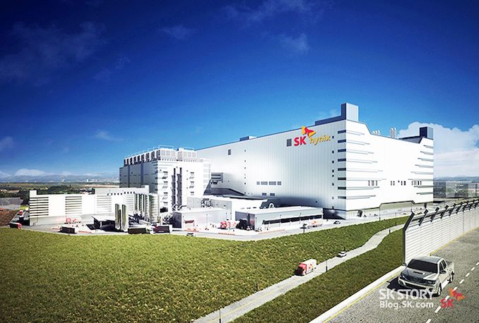
Construction of $106B SK hynix Mega Fab Site Moving Along, But At Slower Pace
Published: Mar 23nd 2024 8:00am on AnandTech
When a major industry slowdown occurs, big companies tend to slowdown their mid-term and long-term capacity related investments. This is exactly what happened to SK hynix's Yongin Semiconductor Cluster, a major project announced in April 2021 and valued at $106 billion. While development of the site has been largely completed, only 35% of the initial shell building has been constructed, according to the Korean Ministry of Trade, Industry, and Energy.
"Approximately 35% of Fab 1 has been completed so far and site renovation is in smooth progress," a statement by the Korean Ministry of Trade, Industry, and Energy reads. "By 2046, over KRW 120 trillion ($90 billion today, $106 billion in 2021) in investment will be poured to complete Fabs 1 through 4, and construction of Fab 1's production line will commence in March next year. Once completed, the infrastructure will rank as the world's largest three-story fab."
The new semiconductor fabrication cluster by SK hynix announced almost exactly three years ago is primarily meant to be used to make DRAM for PCs, mobile devices, and servers using advanced extreme ultraviolet lithography (EUV) process technologies. The cluster, located near Yongin, South Korea, is intended to consist of four large fabs situated on a 4.15 million m2 site. With a planned capacity of approximately 800,000 wafer starts per month (WSPMs), it is set to be one of the world's largest semiconductor production hubs.
With that said, SK hynix's construction progress has been slower than the company first projected. The first fab in the complex was originally meant to come online in 2025, with construction starting in the fourth quarter of 2021. However, SK hynix began to cut its capital expenditures in the second half of 2022, and the Yongin Semiconductor Cluster project fell a victim of that cut. To be sure, the site continues to be developed, just at a slower pace; which is why some 35% of the first fab shell has been built at this point.
If completed as planned in 2021, the first phase of SK hynix Yongin operations would have been a major memory production facility costing $25 billion, equipped with EUV tools, and capable of 200,000-WSPM, according to reports from 2021.
Sources: Korean Ministry of Trade, Industry, and Energy; ComputerBase
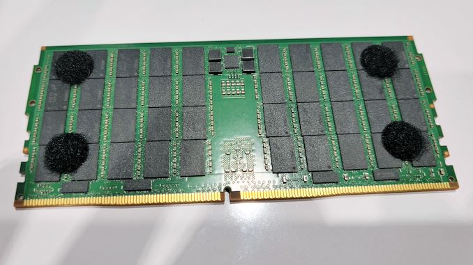
Micron Samples 256 GB DDR5-8800 MCR DIMMs: Massive Modules for Massive Servers
Published: Mar 22nd 2024 4:00am on AnandTech
Micron this week announced that it had begun sampling of its 256 GB multiplexer combined (MCR) DIMMs, the company's highest-capacity memory modules to date. These brand-new DDR5-based MCRDIMMs are aimed at next-generation servers, particularly those powered by Intel's Xeon Scalable 'Granite Rapids' processors that are set to support 12 or 24 memory slots per socket. Usage of these modules can enable datacenter machines with 3 TB or 6 TB of memory, with the combined ranks allowing for effect data rates of DDR5-8800.
"We also started sampling our 256 GB MCRDIMM module, which further enhances performance and increases DRAM content per server," said Sanjay Mehrotra, chief executive of Micron, in prepared remarks for the company's earnings call this week.
In addition to announcing sampling of these modules, Micron also demonstrated them at NVIDIA's GTC conference, where server vendors and customers alike are abuzz at building new servers for the next generation of AI accelerators. Our colleagues from Tom's Hardware have managed to grab a couple of pictures of Micron's 256 GB DDR5-8800 MCR DIMMs.
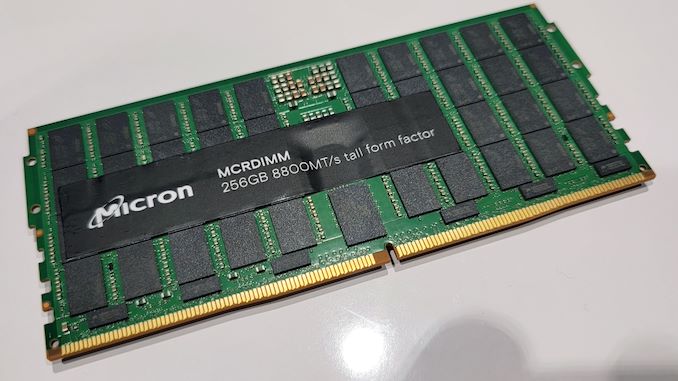
Apparently, Micron's 256 GB DDR5-8800 MCRDIMMs come in two variants: a taller module with 80 DRAM chips distributed on both sides, and a standard-height module using 2Hi stacked packages. Both are based on monolithic 32 Gb DDR5 ICs and are engineered to cater to different server configurations with the standard-height MCRDIMM adressing 1U servers.The taller version consumes about 20W of power, which is in line with expectations as a 128 GB DDR5-8000 RDIMM consumes around 10W in DDR5-4800 mode. I have no idea about power consumption of the version that uses 2Hi packages, though expect it to be a little bit hotter and harder to cool down.
Multiplexer Combined Ranks (MCR) DIMMs are dual-rank memory modules featuring a specialized buffer that allows both ranks to operate simultaneously. This buffer enables the two physical ranks to operate as though they were separate modules working in parallel, which allows for concurrent retrieval of 128 bytes of data from both ranks per clock cycle (compared to 64 bytes per cycle when it comes to regular memory modules), effectively doubling performance of a single module. Of course, since the modules retains physical interface of standard DDR5 modules (i.e., 72-bits), the buffer works with host at a very high data transfer rate to transfer that fetched data to the host CPU. These speeds exceed the standard DDR5 specifications, reaching 8800 MT/s in this case.
While MCR DIMMs make memory modules slightly more complex than regular RDIMMs, they increase performance and capacity of memory subsystem without increasing the number of memory modules involved, which makes it easier to build server motherboards. These modules are poised to play a crucial role in enabling the next generation of servers to handle increasingly demanding applications, particularly in the AI field.
Sources: Tom's Hardware, Micron
Micron Sells Out Entire HBM3E Supply for 2024, Most of 2025
Published: Mar 22nd 2024 11:00am on AnandTech
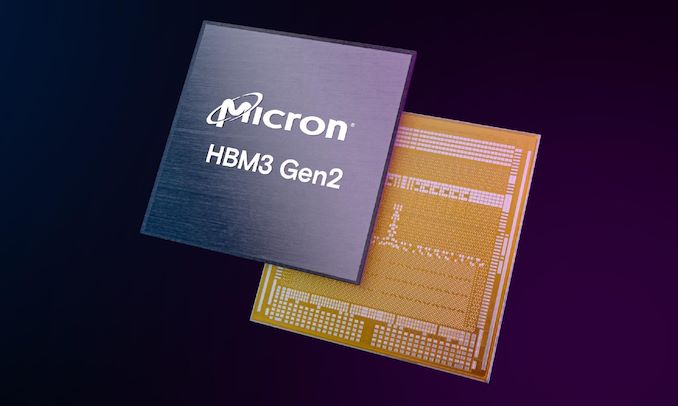
Being the first company to ship HBM3E memory has its perks for Micron, as the company has revealed that is has managed to sell out the entire supply of its advanced high-bandwidth memory or 2024, while most of their 2025 production has been allocated, as well. Micron's HBM3E memory (or how Micron alternatively calls it, HBM3 Gen2) was one of the first to be qualified for NVIDIA's updated H200/GH200 accelerators, so it looks like the DRAM maker will be a key supplier to the green company.
"Our HBM is sold out for calendar 2024, and the overwhelming majority of our 2025 supply has already been allocated," said Sanjay Mehrotra, chief executive of Micron, in prepared remarks for the company's earnings call this week. "We continue to expect HBM bit share equivalent to our overall DRAM bit share sometime in calendar 2025."
Micron's first HBM3E product is an 8-Hi 24 GB stack with a 1024-bit interface, 9.2 GT/s data transfer rate, and a total bandwidth of 1.2 TB/s. NVIDIA's H200 accelerator for artificial intelligence and high-performance computing will use six of these cubes, providing a total of 141 GB of accessible high-bandwidth memory.
"We are on track to generate several hundred million dollars of revenue from HBM in fiscal 2024 and expect HBM revenues to be accretive to our DRAM and overall gross margins starting in the fiscal third quarter," said Mehrotra.
The company has also began sampling its 12-Hi 36 GB stacks that offer a 50% more capacity. These KGSDs will ramp in 2025 and will be used for next generations of AI products. Meanwhile, it does not look like NVIDIA's B100 and B200 are going to use 36 GB HBM3E stacks, at least initially.
Demand for artificial intelligence servers set records last year, and it looks like it is going to remain high this year as well. Some analysts believe that NVIDIA's A100 and H100 processors (as well as their various derivatives) commanded as much as 80% of the entire AI processor market in 2023. And while this year NVIDIA will face tougher competition from AMD, AWS, D-Matrix, Intel, Tenstorrent, and other companies on the inference front, it looks like NVIDIA's H200 will still be the processor of choice for AI training, especially for big players like Meta and Microsoft, who already run fleets consisting of hundreds of thousands of NVIDIA accelerators. With that in mind, being a primary supplier of HBM3E for NVIDIA's H200 is a big deal for Micron as it enables it to finally capture a sizeable chunk of the HBM market, which is currently dominated by SK Hynix and Samsung, and where Micron controlled only about 10% as of last year.
Meanwhile, since every DRAM device inside an HBM stack has a wide interface, it is physically bigger than regular DDR4 or DDR5 ICs. As a result, the ramp of HBM3E memory will affect bit supply of commodity DRAMs from Micron, the company said.
"The ramp of HBM production will constrain supply growth in non-HBM products," Mehrotra said. "Industrywide, HBM3E consumes approximately three times the wafer supply as DDR5 to produce a given number of bits in the same technology node."
NVIDIA's GPU IP Drives into MediaTek's Dimension Auto SoCs
Published: Mar 21nd 2024 5:00am on AnandTech
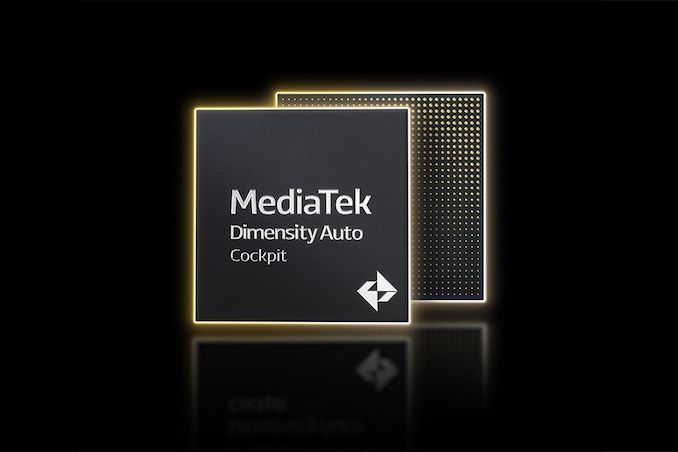
MediaTek this week has introduced a new lineup of Dimensity Auto Cockpit system-on-chips, covering the entire market spectrum from entry-level to premium. And while automotive chip announcements are admittedly not normally the most interesting of things, this one is going to be an exception to that rule because of whose graphics IP MediaTek is tapping for the chips: NVIDIA's. This means the upcoming Dimensity Auto Cockpit chips will be the first chips to be released by a third-party (non-NVIDIA) vendor to be based around NVIDIA's GeForce graphics technology.
NVIDIA's first attempt to license its GPU IP to third parties dates back to the year 2013, when the company proposed to license its Kepler GPU IP and thus rival Arm and Imagination Technologies. An effort that, at the time, landed flat on its face. But over a decade later and a fresh effort at hand to license out some of NVIDIA's IP, and it seems NVIDIA has finally succeeded. Altogether, MediaTek's new Dimensity Auto Cockpit system-on-chips will rely on NVIDIA's GPU IP, Drive OS, and CUDA, setting a historical development for both companies.
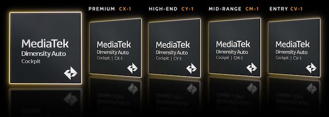
MediaTek's family of next-generation Dimensity Auto Cockpit processors consists of four distinct system-on-chip, including CX-1 for range-topping vehicles, CY-1, CM-1, and CV-1 for entry-level cars. These are highly-integrated SoCs packing Armv9-A-based general-purpose CPU cores as well as NVIDIA's next-generation graphics processing unit IP. NVIDIA's GPU IP can run AI workloads for driver assistance as well as power infotainment system, as it fully supports such graphics technologies like real-time ray-tracing and DLSS 3 image upscaling.
The Dimensity Auto Cockpit processors are monolithic SoCs with built-in multi-camera HDR ISP, according to HardwareLuxx. This ISP supports front-facing, in-cabin, and bird's-eye-view cameras for a variety of safety applications. Additionally, these processors feature an audio DSP that supports various voice assistants.
The announcement from MediaTek does not disclose which generation of NVIDIA's graphics IP they're adopting – only that it's a "next-gen" design. Given the certification requirements involved, automotive SoC announcements tend to be rather conservative, so it remains to be seen just how "next gen" this graphics IP will actually be compared to the current generation Ada Lovelace architecture.
The new MediaTek SoCs will be fully supported by NVIDIA's Drive OS, which is widely used by automakers already. This will allow automakers to unify their software stack and use the same set of software for all of their cars powered by MediaTek's Dimensity. Furthermore, since NVIDIA's Drive OS fully supports CUDA, TensorRT, and Nsight, MediaTek's Dimensity SoCs will be able to take advantage of AI applications developed for the green company's platform.
“Generative AI is transforming the automotive industry in the same way that it has revolutionized the mobile market with more personalized and intuitive computing experiences,” said Jerry Yu, Corporate Senior Vice President and General Manager of MediaTek’s CCM Business Group. “The Dimensity Auto Cockpit portfolio will unleash a new wave of AI-powered entertainment in vehicles, and our unified hardware and software platform makes it easy for automakers to scale AI capabilities across their entire lineup.”
Without a doubt, licensing graphics IP and platform IP to a third party marks a milestone for NVIDIA in general, as well as its automotive efforts in particular. Leveraging DriveOS and CUDA beyond NVIDIA's own hardware platform is a big deal for a business unit that NVIDIA has long considered poised for significant growth, but has faced stiff competition and a slow adoption rate thanks to conservative automakers. Meanwhile, what remains to be seen is how MediaTek's new Dimensity Auto Cockpit processors will stack up against NVIDIA's own previously announced Thor SoC and associated DRIVE Thor platform, which integrates a Blackwell-based GPU delivering 800 TFLOPS of 8-bit floating point AI performance.
AMD Announces FSR 3.1: Seriously Improved Upscaling Quality
Published: Mar 21nd 2024 10:00am on AnandTech
AMD's FidelityFX Super Resolution 3 technology package introduced a plethora of enhancements to the FSR technology on Radeon RX 6000 and 7000-series graphics cards last September. But perfection has no limits, so this week, the company is rolling out its FSR 3.1 technology, which improves upscaling quality, decouples frame generation from AMD's upscaling, and makes it easier for developers to work with FSR.
Arguably, AMD's FSR 3.1's primary enhancement is its improved temporal upscaling image quality: compared to FSR 2.2, the image flickers less at rest and no longer ghosts when in movement. This is a significant improvement, as flickering and ghosting artifacts are particularly annoying. Meanwhile, FSR 3.1 has to be implemented by the game developer itself, and the first title to support this new technology sometime later this year is Ratchet & Clank: Rift Apart.
Temporal Stability AMD FSR 2.2 AMD FSR 3.1 Ghosting Reduction AMD FSR 2.2 AMD FSR 3.1


Another significant development brought by FSR 3.1 is its decoupling from the Frame Generation feature introduced by FSR 3. This capability relies on a form of AMD's Fluid Motion Frames (AFMF) optical flow interpolation. It uses temporal game data like motion vectors to add an additional frame between existing ones. This ability can lead to a performance boost of up to two times in compatible games, but it was initially tied to FSR 3 upscaling, which is a limitation. Starting from FSR 3.1, it will work with other upscaling methods, though AMD refrains from saying which methods and on which hardware for now. Also, the company does not disclose when it is expected to be implemented by game developers.
In addition, AMD is bringing support for FSR3 to Vulkan and Xbox Game Development Kit, enabling game developers on these platforms to use it. It also adds FSR 3.1 to the FidelityFX API, which simplifies debugging and enables forward compatibility with updated versions of FSR.
Upon its release in September 2023, AMD FSR 3 was initially supported by two titles, Forspoken and Immortals of Aveum, with ten more games poised to join them back then. Fast forward to six months later, the lineup has expanded to an impressive roster of 40 games either currently supporting or set to incorporate FSR 3 shortly. As of March 2024, FSR is supported by games like Avatar: Frontiers of Pandora, Starfield, The Last of Us Part I. Shortly, Cyberpunk 2077, Dying Light 2 Stay Human, Frostpunk 2, and Ratchet & Clank: Rift Apart will support FSR shortly.
Source: AMD
Ultra Ethernet Consortium Grows to 55 Members, Reveals Some Details on Upcoming HPC Backbone Tech
Published: Mar 21nd 2024 9:00am on AnandTech

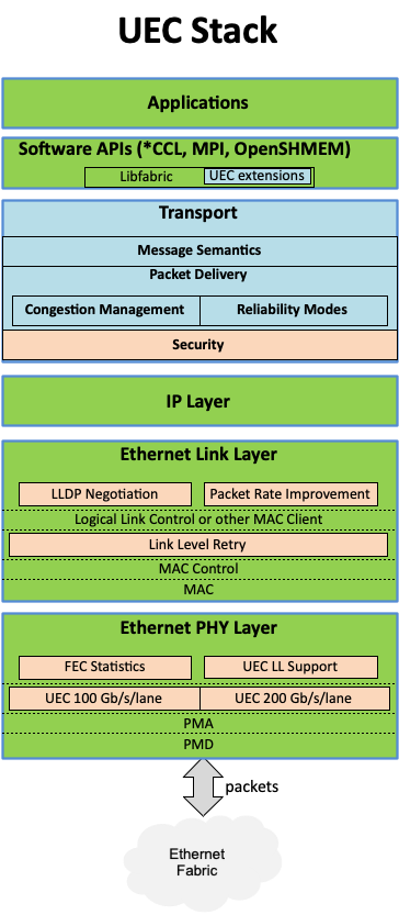
The Ultra Ethernet Consortium (UEC) has announced this week that the next-generation interconnection consortium has grown to 55 members. And as the group works towards developing the initial version of their ultra-fast Ethernet standard, they have released some of the first technical details on the upcoming standard.
Formed in the summer of 2023, the UEC aims to develop a new standard for interconnection for AI and HPC datacenter needs, serving as a de-facto (if not de-jure) alternative to InfiniBand, which is largely under the control of NVIDIA these days. The UEC began to accept new members back in November, and just in five months' time it gained 45 new members, which highlights massive interest for the new technology. The consortium now boasts 55 members and 715 industry experts, who are working across eight technical groups.
There is a lot of work at hand for the UEC, as the group has laid out in their latest development blog post, as the consortium works to to build a unified Ethernet-based communication stack for high-performance networking supporting artificial intelligence and high-performance computing clusters. The consortium's technical objectives include developing specifications, APIs, and source code for Ultra Ethernet communications, updating existing protocols, and introducing new mechanisms for telemetry, signaling, security, and congestion management. In particular, Ultra Ethernet introduces the UEC Transport (UET) for higher network utilization and lower tail latency to speed up RDMA (Remote Direct Memory Access) operation over Ethernet. Key features include multi-path packet spraying, flexible ordering, and advanced congestion control, ensuring efficient and reliable data transfer.
These enhancements are designed to address the needs of large AI and HPC clusters — with separate profiles for each type of deployment — though everything is done in a surgical manner to enhance the technology, but reuse as much of the existing Ethernet as possible to maintain cost efficiency and interoperability.
The consortium's founding members include AMD, Arista, Broadcom, Cisco, Eviden (an Atos Business), HPE, Intel, Meta, and Microsoft. After the Ultra Ethernet Consortium (UEC) began to accept new members in October, 2023, numerous industry heavyweights have joined the group, including Baidu, Dell, Huawei, IBM, Nokia, Lenovo, Supermicro, and Tencent.
The consortium currently plans to release the initial 1.0 version of the UEC specification publicly sometime in the third quarter of 2024.
"There was always a recognition that UEC was meeting a need in the industry," said J Metz, Chair of the UEC Steering Committee. "There is a strong desire to have an open, accessible, Ethernet-based network specifically designed to accommodate AI and HPC workload requirements. This level of involvement is encouraging; it helps us achieve the goal of broad interoperability and stability."
While it is evident that then Ultra Ethernet Consortium is gaining support across the industry, it is still unclear where other industry behemoths like AWS and Google stand. While the hardware companies involved can design Ultra Ethernet support into their hardware and systems, the technology ultimately exists to serve large datacenter and HPC system operators. So it will be interesting to see what interest they take in (and how quickly they adopt) the nascent Ethernet backbone technology once hardware incorporating it is ready.