AMD Announces Ryzen Pro 8000 and Ryzen Pro 8040 Series CPUs: Commercial Desktop Gets AI
Published: Apr 19nd 2024 10:00am on AnandTech
AMD is looking to drive the AI PC market with options across multiple product lines, which aren't limited to consumer processors. While primarily designed for the commercial sector, AMD has announced the Ryzen Pro 8000 'Phoenix' series of APUs for desktops, which AMD claims is the first professional-grade CPU to include an NPU designed to provide on-chip AI neural processing capabilities. AMD has also announced the Ryzen Pro 8040 'Hawk Point' series of mobile processors designed for commercial laptops and notebooks.
AMD's Ryzen Pro 8000 and Ryzen Pro 8040 series processors come with support from AMD's Pro Manageability and AMD Pro Business Ready suites and are built with AMD's current generation Zen 4 cores. The Ryzen Pro 8000 and Ryzen Pro 8040 series processors are similar to their consumer-level counterparts. However, they have additional security features such as AMD Memory Guard, AMD Secure Processor, and Microsoft Pluton.

Touching on the differentiating factors between the non-Pro-consumer chips and the Ryzen Pro series, there is plenty for the commercial and enterprise market regarding security. In what is a first, the Ryzen Pro 8000 series is the first desktop platform to integrate Microsoft Pluton security features designed to protect when connecting to the cloud. Other features include AMD Memory Guard, which encrypts login credentials, keys, and text files stored in the DRAM. AMD Pro Security ties the AMD Zen 4 shadow stack and other layers in directly with the software stack, which, in this case, is Microsoft Windows 11 OS security.
Another notable feature that AMD is hammering home is the on-chip AI capabilities of the included Ryzen AI neural processor unit (NPU), which allows enterprises to run AI workloads locally to mitigate privacy concerns by transferring data to and from the cloud. Although the current generation of NPUs embedded into processors are limited in what they can do, Ryzen AI is a driving factor within the AI PC, as manufacturers and SDVs are looking to utilize AI-accelerated features built into software, such as Microsoft with their AI-powered Copilot tool.
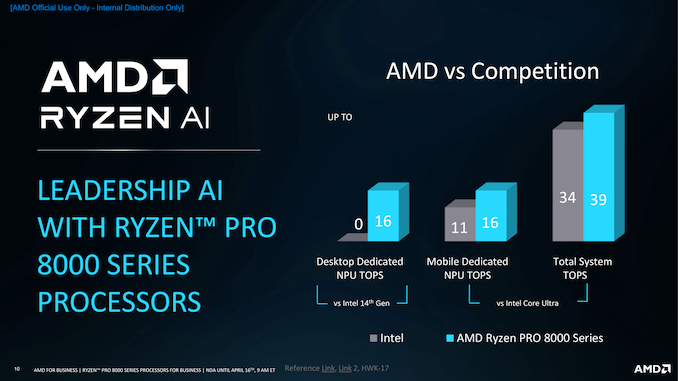
Although there are requirements that now must be met to ensure a PC is considered an 'AI PC,' Microsoft announced that their AI PC requirement is 45 TOPS of performance from the NPU alone, which none of the current generation of chips from AMD and Intel currently meet. In the desktop space, AMD currently has the lead as Intel has presently no offerings with an NPU, although, in the mobile space, AMD with their Ryzen 8040 (Hawk Point) and Intel with their Meteor Lake processors provide plenty of choice for users.
AMD Ryzen Pro 8000 Series (Zen 4) AnandTech Cores Threads Base Freq Boost Freq L3 Cache iGPU TDP Ryzen 7 Pro 8700G 8C / 16T 4200 5100 16 MB R780M (12 CUs) 45-65 W Ryzen 7 Pro 8700GE 8C / 16T 3650 5100 16 MB R780M (12 CUs) 35 W Ryzen 5 Pro 8600G 6C / 12T 4350 5000 16 MB R760M (8 CUs) 45-65 W Ryzen 5 Pro 8500G 6C / 12T 3550 5000 16 MB R740M (4 CUs) 45-65 W Ryzen 5 Pro 8600GE 6C / 12T 3900 5000 16 MB R760M (8 CUs) 35 W Ryzen 5 Pro 8500GE 6C / 12T 3400 5000 16 MB R740M (4 CUs) 35 W Ryzen 3 Pro 8300G 4C / 8T 3450 4900 8 MB R740M (4 CUs) 45-65 W Ryzen 3 Pro 8300GE 4C / 8T 3500 4900 8 MB R740M (4 CUs) 35 WLooking at the AMD Ryzen Pro 8000 series, AMD has announced eight new processors that include the same specifications as the non-Pro Ryzen 8000G APU counterparts. Two primary types of Ryzen Pro 8000 processors are set to be available: four with a configurable TDP of between 45 and 65 W and four with a flat TDP of 35 W for lower-powered environments. Leading the line-up is the Ryzen 7 Pro 8700G, which is identical in core specifications to the Ryzen 7 8700G APU, and has an 8C/16T (Zen 4) configuration with a base frequency of 4.2 GHz and a boost frequency of up to 5.1 GHz.
Even the Ryzen 7 Pro 8700GE, which is the 35 W version, has a 5.1 GHz boost frequency, although it has a slower base clock of 3.65 GHz. Both models have 16 MB of L3 cache, including AMD's integrated Radeon 780M (12 CUs) mobile graphics. All of the eight Ryzen Pro 8000 series models range from 4C/8T offerings with 8 MB of L3 cache and 4.9 GHz boost clocks, 6C/12T models with 5.0 GHz boost clocks and 16 MB of L3 cache, and those as mentioned above 8700/8700GE with 8C/16T.
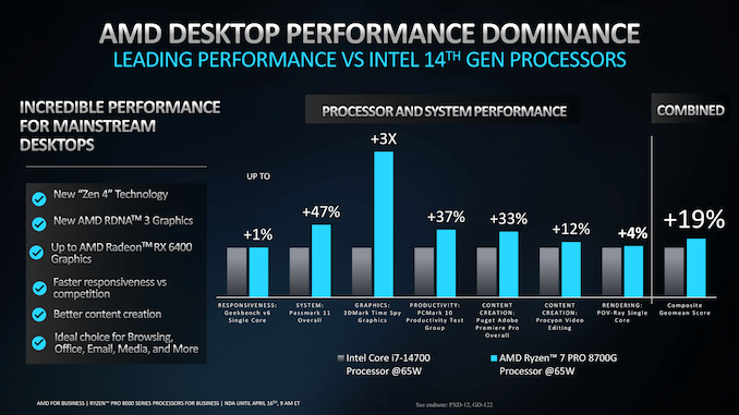
While we take all performance figures given by manufacturers and vendors with a pinch of salt, AMD claims their Ryzen Pro 8000 series offers up to 19% better performance than Intel's 14th-gen Core series processors. AMD's match-up is the Ryzen 7 Pro 8700G vs. the Intel Core i7-14700, with AMD claiming a 47% victory in the Passmark 11 benchmark and 3X the graphics performance in 3D Mark Time Spy. This isn't entirely surprising because the Ryzen 7 Pro 8700G benefits from integrated RDNA3 graphics and AMD's Zen 4 cores.
AMD Ryzen Pro 8040 Series (Zen 4) AnandTech Cores Threads Base Freq Boost Freq L3 Cache iGPU TDP Ryzen 9 Pro 8945HS 8C / 16T 4000 5200 16 MB 12 35-54 W Ryzen 7 Pro 8845HS 8C / 16T 3800 5100 16 MB 12 35-54 W Ryzen 7 Pro 8840HS 8C / 16T 3300 5100 16 MB 12 20-28 W Ryzen 5 Pro 8645HS 6C / 12T 4300 5000 16 MB 8 35-54 W Ryzen 5 Pro 8640HS 6C / 12T 3500 4900 16 MB 8 20-28 W Ryzen 7 Pro 8840U 8C / 16T 3300 5100 16 MB 12 15-28 W Ryzen 5 Pro 8640U 6C / 12T 3500 4900 16 MB 8 15-28 W Ryzen 5 Pro 8540U* 6C / 12T 3200 4900 16 MB 4 15-28 W *Ryzen 5 Pro 8540U is the only chip without AMD's Ryzen AI NPUMoving onto AMD's latest Ryzen Pro 8040 processors for the mobile market, AMD has refreshed their Hawk Point family for the enterprise market. AMD has eight new processors, which are segmented into two families, the HS series and the U series. The HS series has five new chips, which range from 6C/12T up to 8C/16T, all with varying levels of clock speed and TDPs. At the top of the line-up is the Ryzen 9 Pro 8945HS, which is a direct replacement for the Ryzen 9 Pro 7940HS, and as such, it comes with the same 4.0 GHz base clock and 5.2 GHz boost clocks.
Pivitong to TDP, AMD offers the Ryzen 9 Pro 8945HS, Ryzen 7 Pro 8845HS, and Ryzen 5 Pro 8645HS with a configurable TDP of between 35 and 54 W. In contrast, the Ryzen 7 Pro 8840HS and the Ryzen 5 Pro 8640HS are designed for lower-powered laptops with a cTDP of 20-28 W. Regarding cache, all of the announced Ryzen Pro 8040 series models come with 16 MB of L3 Cache. At the same time, specifications such as the integrated graphics and clock speeds all correspond to the consumer line-up, the Ryzen 8040 series.

AMD's in-house performance figures show the Ryzen 7 Pro 8840U at 15 W performing better than Intel's Core Ultra 7 165H at 28 W. Still, as we always do with performance figures provided by vendors, take these with a pinch of salt. AMD claims a 30% combined increase in performance across the board in workloads, including Geekbench v6, Blender, PCMark 10, PCMark Night Raid, and UL Procyon. While there are plenty of different areas where performance gains and losses can be achieved, AMD does claim that their Ryzen 9 Pro 8945HS at 45 W vs. the Intel Core Ultra 9 185H at 45 W is 50% better in Topaz Labs Video AI Gaia 4X software; they did both use discrete graphics in this test according to AMD's slide deck.
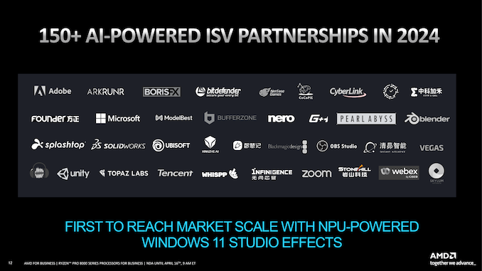
The other notable thing is that all of the Ryzen Pro 8040 series processors, except the bottom SKU, the Ryzen 5 Pro 8540U, come with AMD's Ryzen AI NPU integrated into the silicon. While the AI PC ecosystem is still growing, AMD and over 150+ ISVs look to continue the trend that AI will power more software features in the future than we've seen so far. We are still in the infancy stage of the ecosystem despite much of the marketing targeting the AI functionality, but as we see higher-performing NPUs coming in the next generation of chips, at least ones that can match Microsoft 45 NPU TOPS requirement to run Copilot locally, much of the benefit of the NPU is currently down to how much power can be saved.
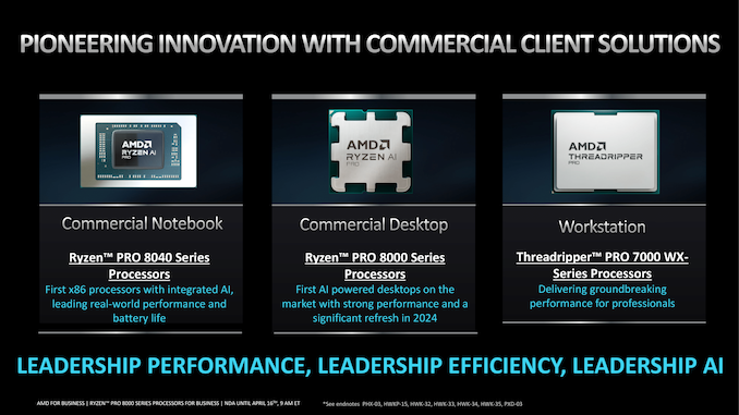
The introduction of the Ryzen Pro 8000/8040 series completes AMD's commercial client platform, along with the readily available Ryzen Threadripper Pro 7000-WX series for commercial and professional workstations. What sets these AMD Ryzen Pro series processors apart from the consumer (non-Pro) variants is support for the AMD Pro Manageability toolkit, which includes features such as cloud-based remote manageability to enable off-site IT technicians the ability to access devices remotely, as well WPA3 SAE encryption, which provides client-to-cloud protection for enterprises over shared networks.
AMD has not announced when the Ryzen Pro 8000 series APUs or the Ryzen Pro 8040 mobile chips will be available for purchase. However, we expect a wide array of OEMs, such as HP and Lenovo, to be already in the process of readying solutions that should hit the market soon.


TSMC Posts Q1'24 Results: 3nm Revenue Share Drops Steeply, but HPC Share Rises
Published: Apr 19nd 2024 8:00am on AnandTech
Taiwan Semiconductor Manufacturing Co. this week released its financial results for Q1 2024. Due to a rebound in demand for semiconductors, the company garned $18.87 billion in revenue for the quarter, which is up 12.9% year-over-year, but a decline of 3.8% quarter-over-quarter. The company says that in increase in demand for HPC processors (which includes processors for AI, PCs, and servers) drove its revenue rebound in Q1, but surprisingly, revenue share of TSMC's flagship N3 (3nm-class) process technology declined steeply quarter-over-quarter.
"Our business in the first quarter was impacted by smartphone seasonality, partially offset by continued HPC-related demand," said Wendell Huang, senior VP and chief financial officer of TSMC. "Moving into second quarter 2024, we expect our business to be supported by strong demand for our industry-leading 3nm and 5nm technologies, partially offset by continued smartphone seasonality."
In the first quarter of 2024, N3 wafer sales accounted for 9% of the foundry's revenue, down from 15% in Q4 2023, and up from 6% in Q3 2023. In terms of dollars, TSMC's 3nm production brought in around $1.698 billion, which is lower than $2.943 billion in the previous quarter. Meanwhile, TSMC's other advanced process technologies increased their revenue share: N5 (5 nm-class) accounted for 37% (up from 35%), and N7 (7 nm-class) commanded 19% (up from 17%). Though both remained relatively flat in terms of revenue, at $6.981 billion and $3.585 billion, respectively.
Generally, advanced technology nodes (N7, N5, N3) generated 65% of TSMC's revenue (down 2% from Q4 2023), while the broader category of FinFET-based process technologies contributed 74% to the company's total wafer revenue (down 1% from the previous quarter).
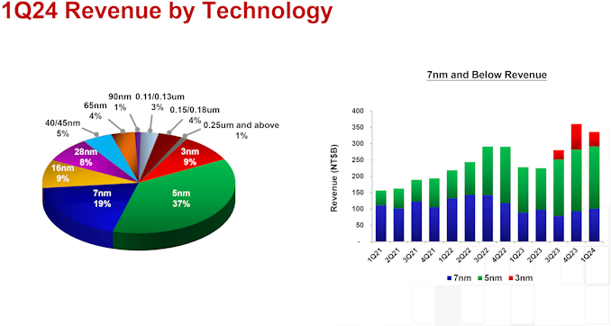
TSMC itself attributes the steep decline of N3's contribution to seasonally lower demand for smartphones in the first quarter as compared to the fourth quarter, which may indeed be the case as demand for iPhones typically slowdowns in Q1. Along those lines, there have also been reports about a drop in demand for the latest iPhones in China.
But even if A17 Pro production volumes are down, Apple remains TSMC's lead customer for N3B, as the fab also produces their M3, M3 Pro, and M3 Max processors on the same node. These SoCs are larger in terms of die sizes and resulting costs, so their contribution to TSMC's revenue should be quite substantial.
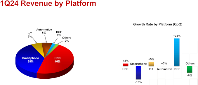
"Moving on to revenue contribution by platform. HPC increased 3% quarter-over-quarter to account for 46% of our first quarter revenue," said Huang. "Smartphone decreased 16% to account for 38%. IoT increased 5% to account for 6%. Automotive remained flat and accounted for 6%, and DCE increased 33% to account for 2%."
Meanwhile, as demand for AI and HPC processors will continue to increase in the coming years, TSMC expects its HPC platform to keep increasing its share in its revenue going forward. "We expect several AI processors to be the strongest driver of our HPC platform growth and the largest contributor in terms of our overall incremental revenue growth in the next several years," said C.C. Wei, chief executive of TSMC.
ASML Patterns First Wafer Using High-NA EUV Tool, Ships Second High-NA Scanner
Published: Apr 18nd 2024 9:00am on AnandTech

This week ASML is making two very important announcements related to their progress with high numerical aperature extreme ultraviolet lithography (High-NA EUV). First up, the company's High-NA EUV prototype system at its fab in Veldhoven, the Netherlands, has printed the first 10nm patterns, which is a major milestone for ASML and their next-gen tools. Second, the company has also revealed that it's second High-NA EUV system is now out the door as well, and has been shipped to an unnamed customer.
"Our High-NA EUV system in Veldhoven printed the first-ever 10 nanometer dense lines," a statement by ASML reads. "Imaging was done after optics, sensors and stages completed coarse calibration. Next up: bringing the system to full performance. And achieving the same results in the field."
Our High NA EUV system in Veldhoven printed the first-ever 10 nanometer dense lines. ✨ Imaging was done after optics, sensors and stages completed coarse calibration. Next up: bringing the system to full performance. And achieving the same results in the field. ⚙️ pic.twitter.com/zcA5V0ScUf
— ASML (@ASMLcompany) April 17, 2024Alongside the system shipped to Intel at the end of 2023, ASML has retained their own Twinscan EXE:5000 scanner at their Veldhoven, Netherlands, facility, which is what the company is using for further research and development into High-NA EUV. Using that machine, the company has been able to print dense lines spaced 10 nanometers apart, which is a major milestone in photolithography development. Previously, only small-scale, experimental lab machines have been able to achieve this kind of a resolution. Eventually, High-NA EUV tools will achieve a resolution of 8 nm, which will be instrumental to build logic chips on technologies beyond 3 nm.
Intel's Twinscan EXE:5000 scanner at its D1X fab near Hillsboro, Oregon is also close behind, and its assembly is said to be nearing completion. That machine will be primarily used for Intel's own High-NA EUV R&D, with Intel slated to use its successor — the commercial-grade Twinscan EXE:5200 — to produce its chips on its Intel 14A (1.4 nm-class) in mass quantities in 2026 – 2027.
But Intel will not be the only chipmaker that gets to experiment with a High-NA EUV scanner for very long. As revealed by ASML, the company recently started shipping another Twinscan EXE:5000 machine to yet another customer. The fab tool maker is not disclosing the client, but previously it has said that all of leading logic and memory producers are in the process of procuring High-NA tools for R&D purposes, so the list of 'suspects' is pretty short.
"Regarding High-NA, or 0.55 NA EUV, we shipped our first system to a customer and this system is currently under installation," said Christophe Fouquet, chief business officer of ASML, at the company's earnings conference call with analysts and investors. "We started to ship the second system this month and its installation is also about to start."
While Intel plans to adopt High-NA EUV tools ahead of the industry, other chipmakers seem to a bit more cautious and plan to rely on risky yet already known Low-NA EUV double patterning method for production a 3 nm and 2 nm. Still, regardless of the exact timing for a transition, all of the major fabs will be relying on High-NA EUV tools in due time. So all parties have an interest in how ASML's R&D turns out.
"The customer interest for our [High-NA] system lab is high as this system will help both our Logic and Memory customers prepare for High-NA insertion into their roadmaps," said Fouquet. "Relative to 0.33 NA, the 0.55 NA system provides finer resolution enabling an almost 3x increase in transistor density, at a similar productivity, in support of sub-2nm Logic and sub-10nm DRAM nodes."
Intel and Sandia National Labs Roll Out 1.15B Neuron “Hala Point” Neuromorphic Research System
Published: Apr 17nd 2024 11:00am on AnandTech

While neuromorphic computing remains under research for the time being, efforts into the field have continued to grow over the years, as have the capabilities of the specialty chips that have been developed for this research. Following those lines, this morning Intel and Sandia National Laboratories are celebrating the deployment of the Hala Point neuromorphic system, which the two believe is the highest capacity system in the world. With 1.15 billion neurons overall, Hala Point is the largest deployment yet for Intel’s Loihi 2 neuromorphic chip, which was first announced at the tail-end of 2021.
The Hala Point system incorporates 1152 Loihi 2 processors, each of which is capable of simulating a million neurons. As noted back at the time of Loihi 2’s launch, these chips are actually rather small – just 31 mm2 per chip with 2.3 billion transistors each, as they’re built on the Intel 4 process (one of the only other Intel chips to do so, besides Meteor Lake). As a result, the complete system is similarly petite, taking up just 6 rack units of space (or as Sandia likes to compare it to, about the size of a microwave), with a power consumption of 2.6 kW. Now that it’s online, Hala Point has dethroned the SpiNNaker system as the largest disclosed neuromorphic system, offering admittedly just a slightly larger number of neurons at less than 3% of the 100 kW British system.
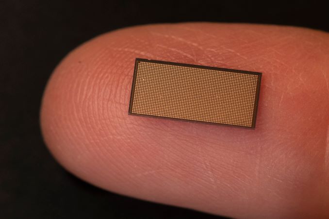 A Single Loihi 2 Chip (31 mm2)
Hala Point will be replacing an older Intel neuromorphic system at Sandia, Pohoiki Springs, which is based on Intel’s first-generation Loihi chips. By comparison, Hala Point offers ten-times as many neurons, and upwards of 12x the performance overall,
Both neuromorphic systems have been procured by Sandia in order to advance the national lab’s research into neuromorphic computing, a computing paradigm that behaves like a brain. The central thought (if you’ll excuse the pun) is that by mimicking the wetware writing this article, neuromorphic chips can be used to solve problems that conventional processors cannot solve today, and that they can do so more efficiently as well.

Sandia, for its part, has said that it will be using the system to look at large-scale neuromorphic computing, with work operating on a scale well beyond Pohoiki Springs. With Hala Point offering a simulated neuron count very roughly on the level of complexity of an owl brain, the lab believes that a larger-scale system will finally enable them to properly exploit the properties of neuromorphic computing to solve real problems in fields such as device physics, computer architecture, computer science and informatics, moving well beyond the simple demonstrations initially achieved at a smaller scale.
One new focus from the lab, which in turn has caught Intel’s attention, is the applicability of neuromorphic computing towards AI inference. Because the neural networks themselves behind the current wave of AI systems are attempting to emulate the human brain, in a sense, there is an obvious degree of synergy with the brain-mimicking neuromorphic chips, even if the algorithms differ in some key respects. Still, with energy efficiency being one of the major benefits of neuromorphic computing, it’s pushed Intel to look into the matter further – and even build a second, Hala Point-sized system of their own.
According to Intel, in their research on Hala Point, the system has reached efficiencies as high as 15 TOPS-per-Watt at 8-bit precision, albeit while using 10:1 sparsity, making it more than competitive with current-generation commercial chips. As an added bonus to that efficiency, the neuromorphic systems don’t require extensive data processing and batching in advance, which is normally necessary to make efficient use of the high density ALU arrays in GPUs and GPU-like processors.
Perhaps the most interesting use case of all, however, is the potential for being able to use neuromorphic computing to enable augmenting neural networks with additional data on the fly. The idea behind this being to avoid re-training, as current LLMs require, which is extremely costly due to the extensive computing resources required. In essence, this is taking another page from how brains operate, allowing for continuous learning and dataset augmentation.
But for the moment, at least, this remains a subject of academic study. Eventually, Intel and Sandia want systems like Hala Point to lead to the development of commercial systems – and presumably, at even larger scales. But to get there, researchers at Sandia and elsewhere will first need to use the current crop of systems to better refine their algorithms, as well as better figure out how to map larger workloads to this style of computing in order to prove their utility at larger scales.CP
Gallery: Intel and Sandia National Laboratories Roll Out “Hala Point” Neuromorphic Research System


Samsung Unveils 10.7Gbps LPDDRX5 Memory - The Fastest Yet
Published: Apr 17nd 2024 10:00am on AnandTech
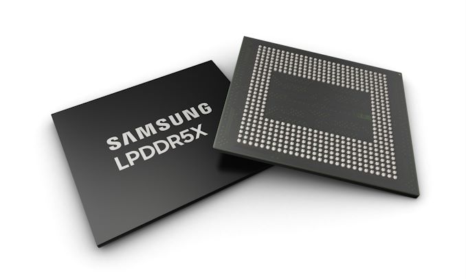
Samsung today has announced that they have developed an even faster generation of LPDDR5X memory that is set to top out at LPDDR5X-10700 speeds. The updated memory is slated to offer 25% better performance and 30% greater capacity compared to existing mobile DRAM devices from the company. The new chips also appear to be tangibly faster than Micron's LPDDR5X memory and SK hynix's LPDDR5T chips.
Samsung's forthcoming LPDDR5X devices feature a data transfer rate of 10.7 GT/s as well as maximum capacity per stack of 32 GB. This allows Samsung's clients to equip their latest smartphones or laptops with 32 GB of low-power memory using just one DRAM package, which greatly simplifies their designs. Samsung says that 32 GB of memory will be particularly beneficial for on-device AI applications.
Samsung is using its latest-generation 12nm-class DRAM process technology to make its LPDDR5X-10700 devices, which allows the company to achieve the smallest LPDDR device size in the industry, the memory maker said.
In terms of power efficiency, Samsung claims that they have integrated multiple new power-saving features into the new LPDDR5X devices. These include an optimized power variation system that adjusts energy consumption based on workload, and expanded intervals for low-power mode that extend the periods of energy saving. These innovations collectively enhance power efficiency by 25% compared to earlier versions, benefiting mobile platforms by extending battery life, the company said.
“As demand for low-power, high-performance memory increases, LPDDR DRAM is expected to expand its applications from mainly mobile to other areas that traditionally require higher performance and reliability such as PCs, accelerators, servers and automobiles,” said YongCheol Bae, Executive Vice President of Memory Product Planning of the Memory Business at Samsung Electronics. “Samsung will continue to innovate and deliver optimized products for the upcoming on-device AI era through close collaboration with customers.”
Samsung plans to initiate mass production of the 10.7 GT/s LPDDR5X DRAM in the second half of this year. This follows a series of compatibility tests with mobile application processors and device manufacturers to ensure seamless integration into future products.
The Iceberg Thermal IceFLOE Oasis 360mm AIO Cooler Review: Affordable & Effective Cooling
Published: Apr 17nd 2024 8:00am on AnandTech
Iceberg Thermal Inc. is one of the newer players in the PC cooling market. The company was founded in 2019 by an experienced team of designers and engineers setting off on their own, aiming to deliver a wide range of PC cooling products to industrial and commercial users alike. They only have a handful of retails products currently available, with the vast majority of them being CPU air coolers, but they have just launched their first liquid cooler products, the IceFLOE Oasis series.
In today’s review, we are having a look at the IceFLOE Oasis 360mm AIO (All-In-One) CPU cooler, the larger of the company's two recently-released liquid coolers. The IceFLOE Oasis CPU cooler targets the high-performance PC cooling market with a sub-$100 price point, aiming to deliver the performance needed to effectively cool a power-hungry processor without being a drain on the wallet in the process. This cooler features a 360mm radiator for an ample heat dissipation area, as well as housing for three high-airflow 120 mm fans. The IceFLOE Oasis supports a wide range of Intel and AMD socket types, making it compatible with a broad spectrum of CPUs. Additionally, it offers advanced RGB lighting, allowing users to customize the aesthetic of their cooling system.
Samsung To Receive $6.4 Billion Under CHIPS Act to Build $40 Billion Fab in Texas
Published: Apr 16nd 2024 5:00am on AnandTech
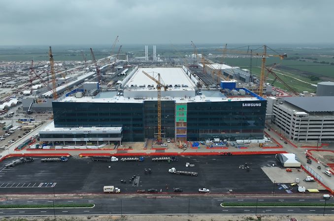
Samsung Electronics this week was awarded up to $6.4 billion from the U.S. government under the CHIPS and Science Act to build its new fab complex in Taylor, Texas. This is the third major award under the act in the last month, with all three leading-edge fabs – Intel, TSMC, and now Samsung – receiving multi-billion dollar funding packages under the domestic chip production program. Overall, the final price tag on Samsung's new fab complex is expected to reach $40 billion by the time it's completed later this decade.
Samsung's CHIPS Act funding was announced during a celebratory event attended by U.S. Secretary of Commerce Gina Raimondo and Samsung Semiconductor chief executive Kye Hyun Kyung. During the event, Kyung outlined the strategic goals of the expansion, emphasizing that the additional funding will not only increase production capacity but also strengthen the entire local semiconductor ecosystem. Samsung plans to equip its fab near Taylor, Texas, with the latest wafer fab tools to produce advanced chips. The Financial Times reports that Samsung aims to produce semiconductors on its 2nm-class process technology starting 2026, though for now this is unofficial information.
"I am pleased to announce a preliminary agreement between Samsung and the Department of Commerce to bring Samsung's advanced semiconductor manufacturing and research and development to Texas," said Joe Biden, the U.S. president, in a statement. "This announcement will unleash over $40 billion in investment from Samsung, and cement central Texas's role as a state-of-the-art semiconductor ecosystem, creating at least 21,500 jobs and leveraging up to $40 million in CHIPS funding to train and develop the local workforce. These facilities will support the production of some of the most powerful chips in the world, which are essential to advanced technologies like artificial intelligence and will bolster U.S. national security."
Samsung has been a significant contributor to the Texas economy for decades, starting chip manufacturing in the U.S. in 1996. With previous investments totaling $18 billion in its Austin operations, Samsung's expansion into Taylor with an additional investment of at least $17 billion underscores its role as one of the largest foreign direct investors in U.S. history. The total expected investment in the new fab surpasses $40 billion, making it one of the largest for a greenfield project in the nation and transforming Taylor into a major hub for semiconductor manufacturing.
The CEO highlighted the substantial economic impact of Samsung's operations, noting a nearly double increase in regional economic output from $13.6 billion to $26.8 billion between 2022 and 2023. The ongoing expansion is projected to further stimulate economic growth, create thousands of jobs, and enhance the community's overall development.
“We are not just expanding production facilities; we’re strengthening the local semiconductor ecosystem and positioning the U.S. as a global semiconductor manufacturing destination.” said Kyung. “To meet the expected surge in demand from U.S. customers, for future products like AI chips, our fabs will be equipped for cutting-edge process technologies and help bring security to the U.S. semiconductor supply chain.”
Samsung is also committed to environmental sustainability and workforce development. The company plans to operate using 100% clean energy and incorporate advanced water management technologies. Additionally, it is investing in education and training programs to develop a new generation of semiconductor professionals. These initiatives include partnerships with educational institutions and programs tailored for military veterans.
In his remarks, Kyung expressed gratitude to President Biden, Secretary Raimondo, and other governmental and community supporters for their ongoing support. This collaborative effort between Samsung and various levels of government, as well as the local community, is pivotal in advancing America's semiconductor industry and ensuring its global competitiveness.
"Today’s announcement will help Samsung bring more semiconductor production, innovation, and jobs to U.S. shores, reinforcing America’s economy, competitiveness, and critical chip supply chains," a statememt by the Semiconductor Industry Associate reads. "We applaud Samsung for investing boldly in U.S.-based manufacturing and salute the U.S. Commerce Department for making significant headway in implementing the CHIPS Act’s manufacturing incentives and R&D programs. We look forward to continuing to work with leaders in government and industry to ensure the CHIPS Act remains on track to help reinvigorate U.S. chip manufacturing and research for many years to come."
NVIDIA Intros RTX A1000 and A400: Entry-Level ProViz Cards Get Ray Tracing
Published: Apr 16nd 2024 12:00am on AnandTech

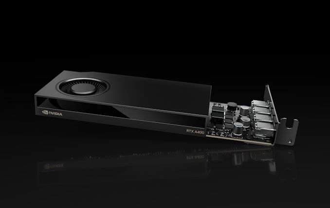
With NVIDIA’s Turing architecture turning six years old this year, the company has been retiring many of the remaining Turing products from its video card lineup. And today that spirit of spring cleaning is coming to the entry-level segment of NVIDIA’s professional visualization lineup, where NVIDIA is introducing a pair of new desktop cards based on their low-end Ampere hardware.
The new RTX A1000 and RTX A400 cards will be replacing the T1000/T600/T400 lineup, which was released three years ago in 2021. The new cards slot into the same entry-level category and finally finish fleshing out the RTX A series of proviz cards, offering NVIDIA’s Ampere-generation professional graphics technologies in the lowest-power, lowest-performance, lowest-cost configuration possible.
Notably, since the entry-level T-series were based on NVIDIA’s feature-limited TU11x silicon, which lacked ray tracing and tensor core support – the basis of NVIDIA’s RTX technologies and associated branding – this marks the first time these technologies will be available in NVIDIA’s entry-level desktop proviz cards. And accordingly, these are being promoted to RTX-branded video cards, ending the odd overlap with NVIDIA’s compute cards, which never carry RTX branding.
It goes without saying that as low-end cards, the ray tracing performance of either part is nothing to write home about, but it gives NVIDIA’s current proviz lineup a consistent set of graphics features from top to bottom.
NVIDIA Professional Visualization Card Specification Comparison A1000 A400 T1000 T400 CUDA Cores 2304 768 896 384 Tensor Cores 72 24 N/A N/A Boost Clock 1460MHz 1755MHz 1395MHz 1425MHz Memory Clock 12Gbps GDDR6 12Gbps GDDR6 10Gbps GDDR6 10Gbps GDDR6 Memory Bus Width 128-bit 64-bit 128-bit 64-bit VRAM 8GB 4GB 8GB 4GB Single Precision 6.74 TFLOPS 2.7 TFLOPS 2.5 TFLOPS 1.09 TFLOPS Tensor Performance 53.8 TFLOPS 21.7 TFLOPS N/A N/A TDP 50W 50W 50W 30W Cooling Active, SS Active, SS Active, SS Active, SS Outputs 4x mDP 1.4a 4x mDP 1.4a 3x mDP 1.4a GPU GA107 TU117 Architecture Ampere Turing Manufacturing Process Samsung 8nm TSMC 12nm Launch Date 04/2024 05/2024 05/2021 05/2021Both the A1000 and A400 are based on the same board design, with NVIDIA doing away with any pretense of physical feature differentiation this time around (T400 was missing its 4th Mini DisplayPort). This means both cards are based on the GA107 GPU, sporting different core and memory configurations.
RTX A1000 is a not-quite-complete configuration of GA107, with 2304 CUDA cores and 72 tensor cores. This is paired with 8GB of GDDR6, which runs at 12Gbps, for a total of 192GB/second of memory bandwidth. The TDP of the card is 50 Watts, matching its predecessor.
Meanwhile RTX A400 is far more cut down, offering about a third of the active hardware on the GPU itself, and half the memory bandwidth. On paper this gives it around 40% of T1000’s performance, and half the memory bandwidth – or 96GB/second. Notably, despite the hardware cut-down, the official TDP is still 50 Watts, versus the 30 Watts of its predecessor. So at this point NVIDIA will soon cease offering a desktop proviz card lower than 50 Watts.
As noted before, both cards otherwise feature the same physical design, with a half-height half-length (HHHL) board with active cooling. As you’d expect from such low-TDP cards, these are single-slot cooler designs. Both cards feature a quartet of Mini DisplayPorts, with the same DP 1.4a functionality that we’ve seen across all of NVIDIA’s products for the last several years.
Finally, video-focused users will want to make note that the A1000/A400 have slightly different video capabilities. While A1000 gets access to both of GA107’s NVDEC video decode blocks, A400 only gets access to a single block – one more cutback to differentiate the two cards. Otherwise, both video cards get access to the GPU’s sole NVENC block.
According to NVIDIA, the RTX A1000 will be available starting today through its distribution partners. Meanwhile the RTX A400 will hit distribution channels in May, and with OEMs expected to begin offering the cards as part of their pre-built systems this summer.
SK hynix Tube T31 Stick SSD Review: Bridging Solution Springs A Surprise
Published: Apr 15nd 2024 8:00am on AnandTech
SK hynix is one of the few vertically integrated manufacturers in the flash-based storage market. The company is well-established in the OEM market. A few years back, they also started exploring direct end-user products. Internal SSDs (starting with the Gold S31 and Gold P31) were the first out of the door. Late last year, the company introduced the Beetle X31 portable SSD, its first direct-attached storage product. In February, a complementary product was introduced - the Tube T31 Stick SSD.
The Beetle X31 is a portable SSD with a Type-C upstream port and a separate cable. The Tube T31 is a take on the traditional thumb drive with a male Type-A interface. The size of the Beetle X31 makes the use of a bridge solution obvious. Our investigation into the Tube T31 also revealed the use of the same internal SSD, albeit with a different bridge. Read on for a detailed look at the Tube T31, including an analysis of its internals and evaluation of its performance consistency, power consumption, and thermal profile.
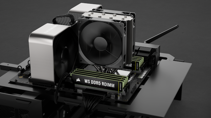
Corsair Enters Workstation Memory Market with WS Series XMP/EXPO DDR5 RDIMMs
Published: Apr 12nd 2024 8:30am on AnandTech
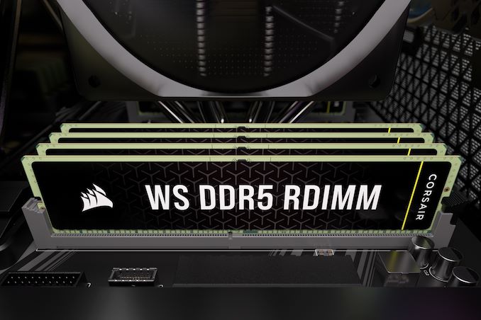
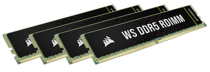
Corsair has introduced a family of registered memory modules with ECC that are designed for AMD's Ryzen Threadripper 7000 and Intel's Xeon W-2400/3400-series processors. The new Corsair WS DDR5 RDIMMs with AMD EXPO and Intel XMP 3.0 profiles will be available in kits of up to 256 GB capacity and at speeds of up to 6400 MT/s.
Corsair's family of WS DDR5 RDIMMs includes 16 GB modules operating at up to 6400 MT/s with CL32 latency as well as 32 GB modules functioning at 5600 MT/s with CL40 latency. At present, Corsair offers a quad-channel 64 GB kit (4×16GB, up to 6400 MT/s), a quad-channel 128GB kit (4×32GB, 5600 MT/s), an eight-channel 128 GB kit (8×16GB, 5600 MT/s), and an eight-channel 256 GB kit (8×32GB, 5600 MT/s) and it remains to be seen whether the company will expand the lineup.
Corsair's WS DDR5 RDIMMs are designed for AMD's TRX50 and WRX90 platforms as well as Intel's W790 platform and are therefore compatible with AMD's Ryzen Threadripper Pro 7000 and 7000WX-series as well as Intel's Xeon W-2400/3400-series CPUs. The modules feature both AMD EXPO and Intel XMP 3.0 profiles to easily set their beyond-JEDEC-spec settings and come with thin heat spreaders made of pyrolytic graphite sheet (PGS), which thermal conductivity than that of copper and aluminum of the same thickness. For now, Corsair does not disclose which RCD and memory chips its registered memory modules use.
Unlike many of its rivals among leading DIMM manufacturers, Corsair did not introduce its enthusiast-grade RDIMMs when AMD and Intel released their Ryzen Threadripper and Xeon W-series platforms for extreme workstations last year. It is hard to tell what the reason for that is, but perhaps the company wanted to gain experience working with modules featuring registered clock drivers (RCDs) as well as AMD's and Intel's platforms for extreme workstations.
The result of the delay looks to be quite rewarding: unlike modules from its competitors that either feature AMD EXPO or Intel XMP 3.0 profiles, Corsair's WS DDR5 RDIMMs come with both. While this may not be important on the DIY market where people know exactly what they are buying for their platform, this is a great feature for system integrators, which can use Corsair WS DDR5 RDIMMs both for their AMD Ryzen Threadripper and Intel Xeon W-series builds, something that greatly simplifies their inventory management.
Since Corsair's WS DDR5 RDIMMs are aimed at workstations and are tested to offer reliable performance beyond JEDEC specifications, they are quite expensive. The cheapest 64 GB DDR5-5600 CL40 kit costs $450, the fastest 64 GB DDR5-6400 CL32 kit is priced at $460, whereas the highest end 256 GB DDR5-5600 CL40 kit is priced at $1,290.