TSMC 2nm Update: N2 In 2025, N2P Loses Backside Power, and NanoFlex Brings Optimal Cells
Published: Apr 25nd 2024 8:30am on AnandTech
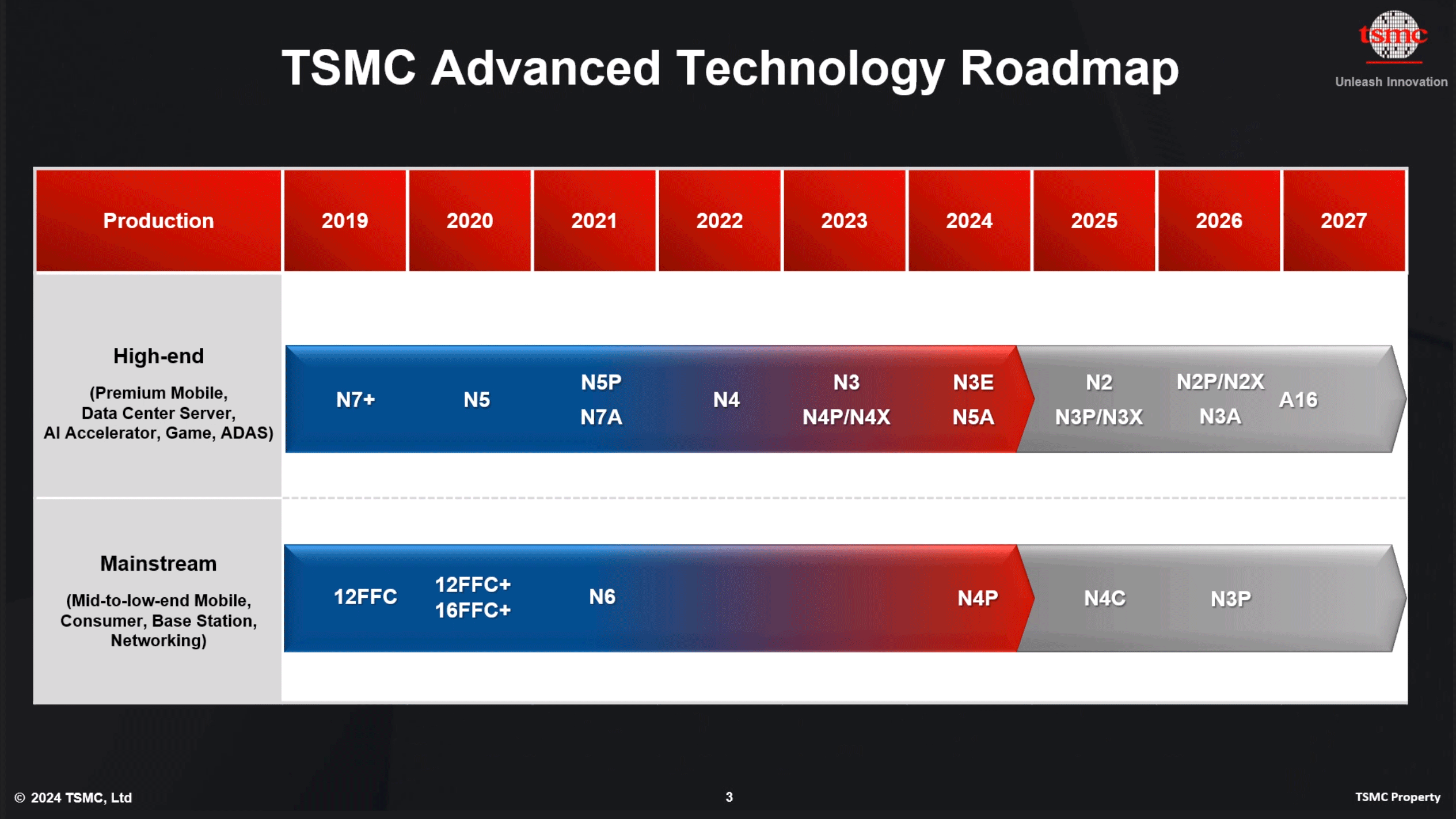
Taiwan Semiconductor Manufacturing Co. provided several important updates about its upcoming process technologies at its North American Technology Symposium 2024. At a high level, TSMC's 2 nm plans remain largely unchanged: the company is on track to start volume production of chips on it's first-generation GAAFET N2 node in the second half of 2025, and N2P will succeed N2 in late 2026 – albeit without the previously-announced backside power delivery capabilities. Meanwhile, the whole N2 family will be adding TSMC's new NanoFlex capability, which allows chip designers to mix and match cells from different libraries to optimize performance, power, and area (PPA).
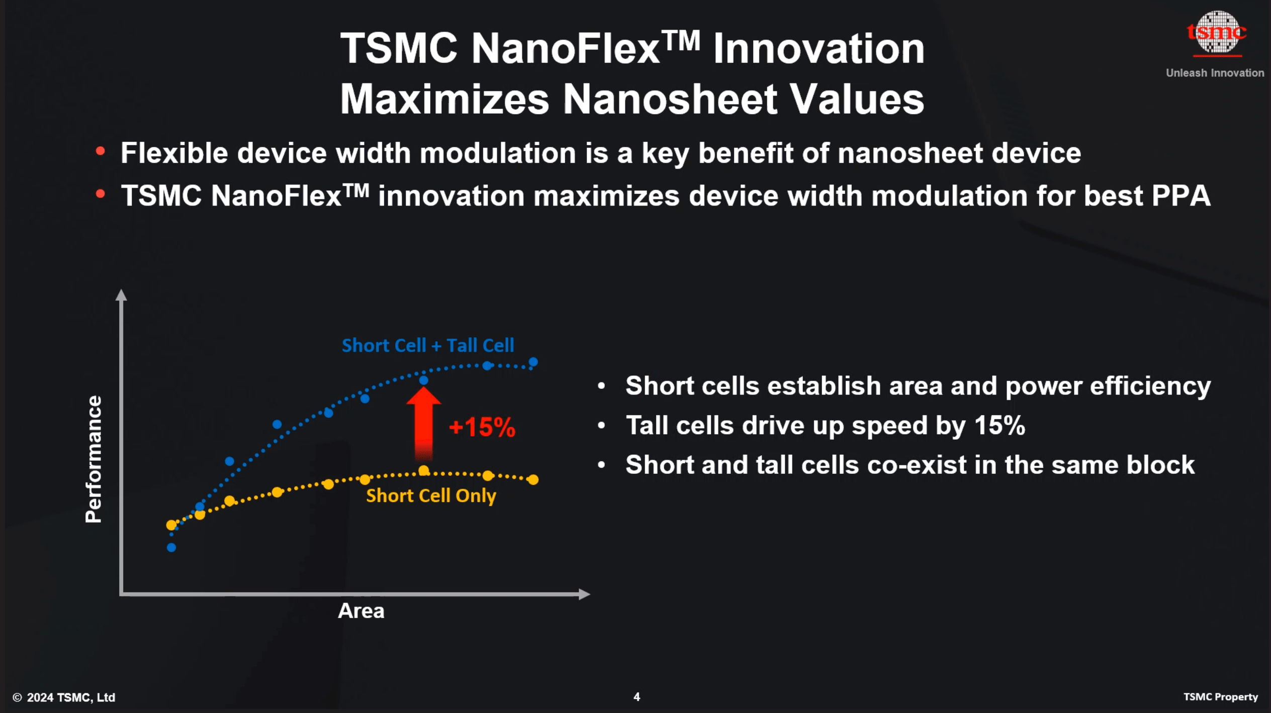
One of the key announcements of the event is TSMC's NanoFlex technology, which will be a part of the company's complete N2 family of production nodes (2 nm-class, N2, N2P, N2X). NanoFlex will enable chip designers to mix and match cells from different libraries (high performance, low power, area efficient) within the same block design, allowing designers to fine tune their chip designs to improve performance or lower power consumption.
TSMC's contemporary N3 fabrication process already supports a similar capability called FinFlex, which also allows designers to use cells from different libraries. But since N2 relies on gate-all-around (GAAFET) nanosheet transistors, NanoFlex gives TSMC some additional controls: firstly, TSMC can optimize channel width for performance and power and then build short cells (for area and power efficiency) or tall cells (for up to 15% higher performance).
When it comes to timing, TSMC's N2 is set to enter risk production in 2025 and high-volume manufacturing (HVM) in the second half of 2025, so it looks like we are going to see N2 chips in retail devices in 2026. Compared to N3E, TSMC expects N2 to increase performance by 10% to 15% at the same power, or reduce power consumption by 25% to 30% at the same frequency and complexity. As for chip density, the foundry is looking at a 15% density increase, which is a good degree of scaling by contemporary standards.
N2 will be followed by performance-enhanced N2P, as well as the voltage-enhanced N2X in 2026. Although TSMC once said that N2P would add backside power delivery network (BSPDN) in 2026, it looks like this will not be the case and N2P will use regular power delivery circuitry. The reason for this is unclear, but it looks like the company decided not to add a costly feature to N2P, but to reserve it to its next-generation node, which will also be available to customers in late 2026.
N2 is still expected to feature a major innovation related to power: super-high-performance metal-insulator-metal (SHPMIM) capacitors, which are are being added to improve power supply stability. The SHPMIM capacitor offers more than twice the capacity density of TSMC's existing super-high-density metal-insulator-metal (SHDMIM) capacitor. Additionally, the new SHPMIM capacitor cuts sheet resistance (Rs in Ohm/square) and via resistance (Rc) by 50% compared to its predecessor.
Related ReadingTSMC's 1.6nm Technology Announced for Late 2026: A16 with "Super Power Rail" Backside Power
Published: Apr 25nd 2024 7:30am on AnandTech
With the arrival of spring comes showers, flowers, and in the technology industry, TSMC's annual technology symposium series. With customers spread all around the world, the Taiwanese pure play foundry has adopted an interesting strategy for updating its customers on its fab plans, holding a series of symposiums from Silicon Valley to Shanghai. Kicking off the series every year – and giving us our first real look at TSMC's updated foundry plans for the coming years – is the Santa Clara stop, where yesterday the company has detailed several new technologies, ranging from more advanced lithography processes to massive, wafer-scale chip packing options.
Today we're publishing several stories based on TSMC's different offerings, starting with TSMC's marquee announcement: their A16 process node. Meanwhile, for the rest of our symposium stories, please be sure to check out the related reading below, and check back for additional stories.
Headlining its Silicon Valley stop, TSMC announced its first 'angstrom-class' process technology: A16. Following a production schedule shift that has seen backside power delivery network technology (BSPDN) removed from TSMC's N2P node, the new 1.6nm-class production node will now be the first process to introduce BSPDN to TSMC's chipmaking repertoire. With the addition of backside power capabilities and other improvements, TSMC expects A16 to offer significantly improved performance and energy efficiency compared to TSMC's N2P fabrication process. It will be available to TSMC's clients starting H2 2026.
TSMC A16: Combining GAAFET With Backside Power DeliveryAt a high level, TSMC's A16 process technology will rely on gate-all-around (GAAFET) nanosheet transistors and will feature a backside power rail, which will both improve power delivery and moderately increase transistor density. Compared to TSMC's N2P fabrication process, A16 is expected to offer a performance improvement of 8% to 10% at the same voltage and complexity, or a 15% to 20% reduction in power consumption at the same frequency and transistor count. TSMC is not listing detailed density parameters this far out, but the company says that chip density will increase by 1.07x to 1.10x – keeping in mind that transistor density heavily depends on the type and libraries of transistors used.
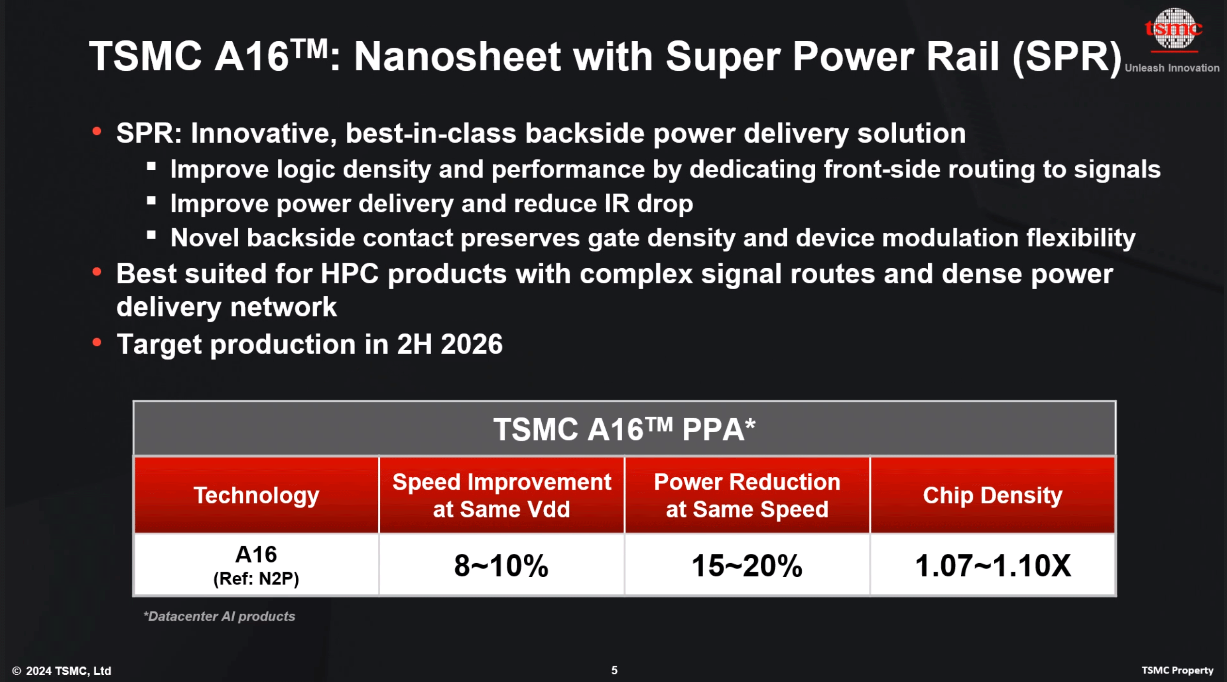
The key innovation of TSMC's A16 node, is its Super Power Rail (SPR) backside power delivery network, a first for TSMC. The contract chipmaker claims that A16's SPR is specifically tailored for high-performance computing products that feature both complex signal routes and dense power circuitry.
As noted earlier, with this week's announcement, A16 has now become the launch vehicle for backside power delivery at TSMC. The company was initially slated to offer BSPDN technology with N2P in 2026, but for reasons that aren't entirely clear, the tech has been punted from N2P and moved to A16. TSMC's official timing for N2P in 2023 was always a bit loose, so it's hard to say if this represents much of a practical delay for BSPDN at TSMC. But at the same time, it's important to underscore that A16 isn't just N2P renamed, but rather it will be a distinct technology from N2P.
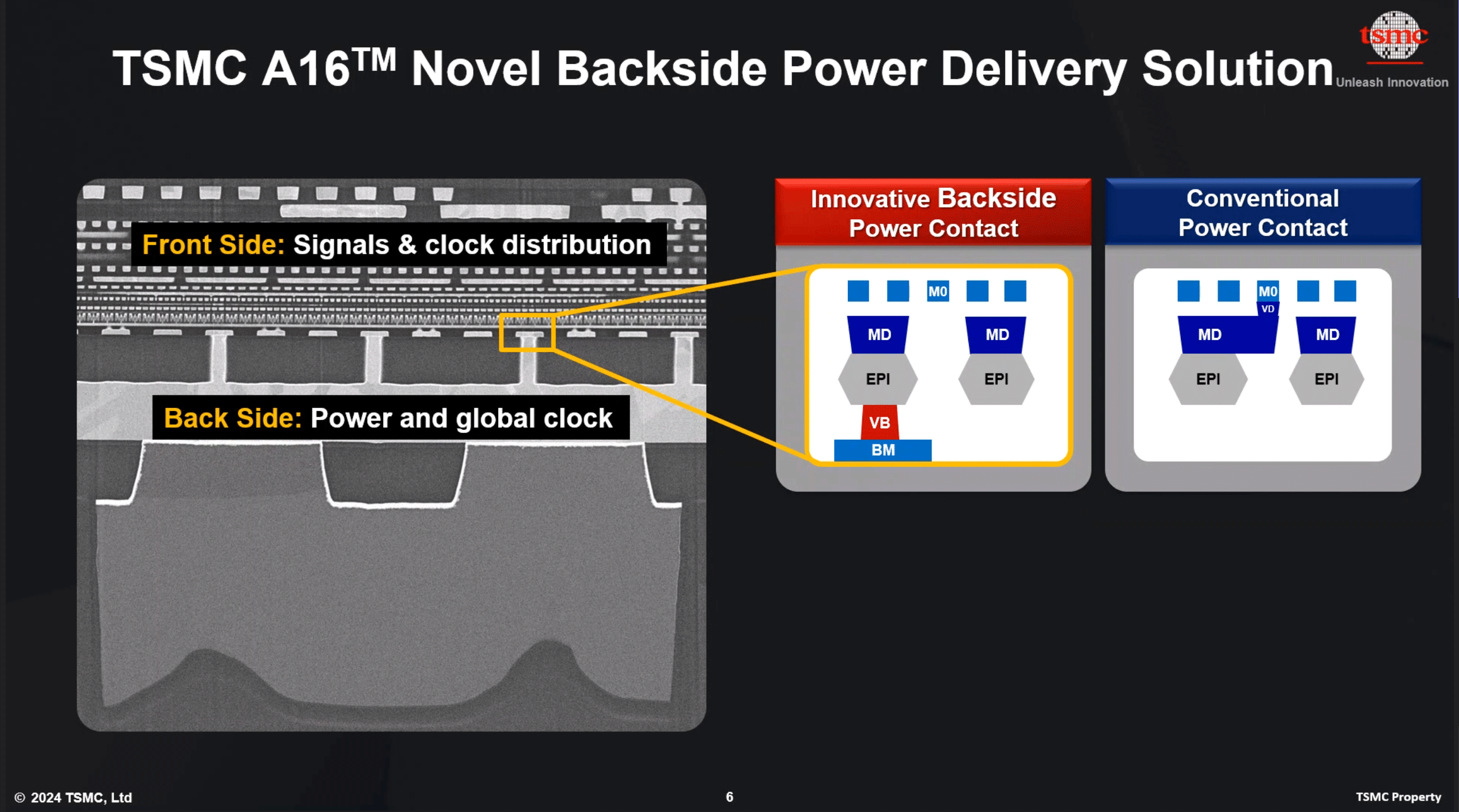
TSMC is not the only fab pursuing backside power delivery, and accordingly, we're seeing multiple variations on the technique crop up at different fabs. The overall industry has three approaches for BSPDN: Imec's Buried Power Rail, Intel's PowerVia, and now TSMC's Super Power Rail.
The oldest technique, Imec's Buried Power Rail, essentially places power delivery network on the backside of the wafer and then connects power rail of logic cells to power contact using nano TSVs. This enables some area scaling and does not add too much complexity to production. The second implementation, Intel's PowerVia, connects power to the cell or transistor contact, which provides a better result, but at the cost of complexity.
Finally, we have TSMC's new Super Power Rail BSPDN technology, which connects a backside power network directly to each transistor's source and drain. According to TSMC, this is the most efficient technology in terms of area scaling, but the trade-off is that it's the most complex (and expensive) when it comes to production.
That TSMC has opted to go with the most complex version of BSPDN may be part of the reason that we've seen it removed from N2P, as implementing it will ultimately add to both time and costs. This leaves A16 as TSMC's premiere performance node for the 2026/2027 time-frame, while N2P can be positioned to offer a more balanced combination of performance and cost efficiency.
Angstrom Era Kicks Off In Late 2026 With New Node Naming ConventionFinally, as with Intel, we're also seeing TSMC adopt a new process node naming convention starting with this generation of technology. The name itself is largely arbitrary – and this has already been the case in the fab industry for several years now – but with current node names already in the single digits (e.g. N2), the industry has needed to re-calibrate node names to something smaller than the nanometer. And thus we've arrived at the 'angstrom era.' But regardless of what exactly it's called or why it's called that, the important point is that A16 will be the next generation node beyond TSMC's 2nm-class products.
TSMC expects to start volume production on A16 in H2 2026, so it is likely that the first products based on this technology will hit the market in 2027. Given the timing, the production node will presumably compete against Intel's 14A; though at 2+ years out and with no one producing BSPDN in volume today, there's still a lot of time for plans and roadmaps to change.
Report: Seagate, Western Digital Hike HDD Prices Amid Surge In Demand
Published: Apr 24nd 2024 12:00am on AnandTech
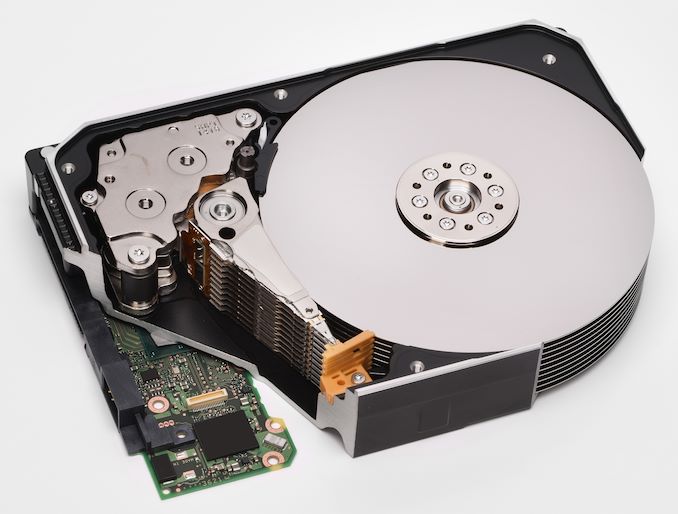
Seagate Technology has reportedly notified its customers abouts its plans to raise prices on new hard drive orders and for demands that exceed prior agreements, echoing a similar move by Western Digital, which increased its prices earlier this month. These changes come in response to a surge in demand for high-capacity HDDs and constraints in supply due to decreased production capabilities of both Seagate and Western Digital, reports TrendForce.
According to industry insights reported by TechNews, the sector anticipates that the scarcity of high-capacity HDD products will persist throughout the current quarter and possibly extend over the entire year. It is forecasted that HDD prices will rise by 5% to 10% in Q2 2024 alone and could increase further as a reault of the ongoing challenges faced by the storage industry.
The primary driver behind Seagate's decision is increased demand for high-capacity HDDs, which are used to train AI models. This demand spike, coupled with a reduction in production output from hard drive makers, has created a significant supply-demand imbalance. As a result, Seagate has decided to adjust their pricing strategy to manage the situation. Further exacerbating the issue are global inflationary pressures which continue to inflate costs across the board, which also contributed to the company's decision to increase prices, Seagate said in a message to clients published by TrendForce.
Seagate emphasized that its reduced production capacity has been a major challenge, hindering the company's ability to fulfill customer demands fully and promptly.
"As a result, we will be implementing price increases effective immediately on new orders and for demand that is over and above previously committed volumes," the alleged memo from Seagate reads. "Supply constraints are expected to continue and as such we anticipate that prices will continue to increase in the coming quarters."
Earlier this month Western Digital also informed its customers about price hikes for its HDD and SSD products. This notification was based on similar issues — higher than anticipated demand across the whole product range and additional supply chain challenges affecting the electronics sector. Western Digital's announcement made it clear that these disruptions are likely to continue, prompting further price adjustments.
Sources: TrendForce, TrendForce, TechNews
Qualcomm Intros Snapdragon X Plus, Details Complete Snapdragon X Launch Day Chip Stack
Published: Apr 24nd 2024 9:15am on AnandTech
As Qualcomm prepares for the mid-year launch of their forthcoming Snapdragon X SoCs for PCs, and the eagerly anticipated Oryon CPU cores within, the company is finally shoring up their official product plans, and releasing some additional technical details in the process. Thus far the company has been demonstrating their Snapdragon X Elite SoC in its highest-performing, fully-enabled configuration. But the retail Snapdragon X Elite will not be a single part; instead, Qualcomm is preparing a whole range of chip configurations for various price/performance tiers in the market. Altogether, there will be 3 Snapdragon X Elite SKUs that differ in CPU and GPU performance.
As well, the company is introducing a second Snapdragon X tier, Snapdragon X Plus, for those SKUs positioned below the Elite performance tier. As of today, this will be a single configuration. But if the Snapdragon X lineup is successful and demand warrants it, I would not be surprised to see Qualcomm expand it further – as they have certainly left themselves the room for it in their product stack. In the meantime, with Qualcomm’s expected launch competition now shipping (Intel Core Ultra Meteor Lake and AMD Ryzen Mobile 8040 Hawk Point), the company is also very confident that even these reduced performance Snapdragon X Plus chips will be able to beat Intel and AMD in multithreaded performance – never mind the top-tier Snapdragon X Elite chips.
Qualcomm will be launching this expanded four chip stack at once; so both Snapdragon X Elite and Snapdragon X Plus tier devices should be available at the same time. The company’s goal is still to have devices on the shelf “mid-year”, although the company isn’t providing any more precise guidance than that. With Qualcomm’s CEO, Cristiano Amon, set to deliver a Computex keynote in June, I expect we’ll get more specific details on timings then, along with the company and its partners using the event to announce and showcase some retail laptop designs. So this is very much looking like a summer launch at the moment.
In the meantime, Qualcomm is already showing off what their Snapdragon X Plus chips can do with a fresh set of live benchmarks, akin to their Snapdragon X Elite performance previews from October 2023. We’ll dive into those in a bit, but suffice it to say, Qualcomm knows the score, and they want to make sure the entire world knows when they’re winning.
Seagate: Mozaic 3+ HAMR Hard Drives Can Last Over Seven Years
Published: Apr 23nd 2024 7:30am on AnandTech
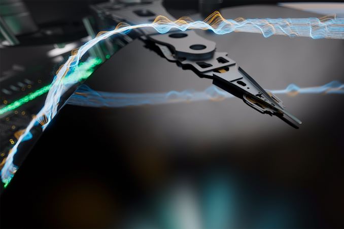
As Seagate ramps up shipments of its new heat assisted magnetic recording (HAMR)-based Mozaic 3+ hard drive platform, the company is both in the enviable position of shipping the first major new hard drive technology in a decade, and the much less enviable position of proving the reliability of the first major new hard drive technology in a decade. Due to HAMR's use of temporal heating with its platters, as well as all-new read/write heads, HAMR introduces multiple new changes at once that have raise questions about how reliable the technology will be. Looking to address these matters (and further promote their HAMR drives), Seagate has published a fresh blog post outlining the company's R&D efforts, and why the company expects their HAMR drives to last several years – as long or longer than current PMR hard drives.
According to the company, the reliability of Mozaic 3+ drives on par with traditional drives relying on perpendicular magnetic recording (PMR), the company says. In fact, components of HAMR HDDs have demonstrated a 50% increase in reliability over the past two years. Seagate says that Mozaic 3+ drives boast impressive durability metrics: their read/write heads have demonstrated capacity to handle over 3.2 petabytes of data transfer over 6,000 hours of operation, which exceeds data transfers of typical nearline hard drives by 20 times. Accordingly, Seagate is rating these drives for a mean time between failure (MTBF) 2.5 million hours, which is in-line with PMR-based drives.
Based on their field stress tests, involving over 500,000 Mozaic 3+ drives, Seagate says that the heads of Mozaic 3+ drives will last over seven years, surpassing the typical lifespan of current PMR-based drives. Generally, customers anticipate that modern PMR drives will last between four and five years with average usage, so these drives would exceed current expectations.
Altogether, Seagate is continuing aim for a seamless transition from PMR to HAMR drives in customer systems. That means ensuring that these new drives can fit into existing data center infrastructures without requiring any changes to enterprise specifications, warranty conditions, or form factors.
Samsung Starts Mass Production of 9th Generation V-NAND: 1Tb 3D TLC NAND
Published: Apr 23nd 2024 6:30am on AnandTech
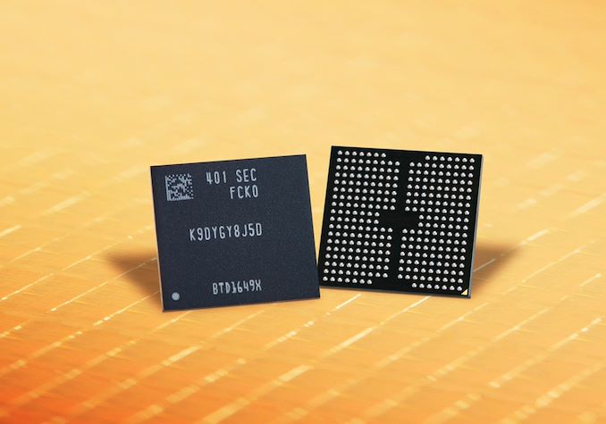
Samsung Electronics has started mass production of its 9th generation of V-NAND memory. The first dies based on their latest NAND tech come in a 1 Tb capacity using a triple-level cell (TLC) architecture, with data transfer rates as high as 3.2 GT/s. The new 3D TLC NAND memory will initially be used to build high-capacity and high-performance SSDs, which will help to solidify Samsung's position in the storage market.
Diving right in, Samsung is conspicuously avoiding to list the number of layers in their latest generation NAND, which is the principle driving factor in increasing capacity generation-on-generation. The company's current 8th gen V-NAND is 236 layers – similar to its major competitors – and word on the street is that 9th gen V-NAND ups that to 290 layers, though this remains to be confirmed.
Regardless, Samsung says that its 9th generation V-NAND memory boasts an approximate 50% improvement in bit density over its 8th generation predecessor. Driving this gains, the company cites the miniaturization of the cell size, as well as the integration of enhanced memory cell technologies that reduce interference and extend the lifespan of the cells. With their latest NAND technology, Samsung has also been able to eliminate dummy channel holes, thus reducing the planar area of the memory cells.
Interestingly, today's announcement also marks the first time that Samsung has publicly confirmed their use of string stacking in their NAND, referring to it as their "double-stack structure." The company is widely believed to have been using sting stacking back in their 8th generation NAND as well, however this was never confirmed by the company. Regardless, the use of string stacking is only going to increase from here, as vendors look to keep adding layers to their NAND dies, while manufacturing variability and channel hole tolerances make it difficult to produce more than 150-200 layers in a single stack.
Samsung TLC V- NAND Flash Memory 9th Gen V-NAND 8th Gen V-NAND Layers 290? 236 Decks 2 (x145) 2 (x118) Die Capacity 1 Tbit 1 Tbit Die Size (mm2) ?mm2 ?mm2 Density (Gbit/mm2) ? ? I/O Speed 3.2 GT/s (Toggle 5.1) 2.4 GT/s (Toggle 5.0) Planes 6? 4 CuA / PuC Yes YesSpeaking of channel holes, another key technological enhancement in the 9th gen V-NAND is Samsung's advanced 'channel hole etching' technology. This process improves manufacturing productivity by enabling the simultaneous creation of electron pathways within a double-stack structure. This method is crucial as it enables efficient drilling through more layers, which is increasingly important as cell layers are added.
The latest V-NAND also features the introduction of a faster NAND flash interface, Toggle DDR 5.1, which boosts peak data transfer rates by 33% to 3.2 GT/s, or almost 400MB/sec for a single die. Additionally, 9th gen V-NAND's power consumption has been reduced by 10%, according to Samsung. Though Samsung doesn't state under what conditions – presumably, this is at iso-frequency rather than max frequency.
Samsung's launch of 1Tb TLC V-NAND is set to be followed by the release of a quad-level cell (QLC) model later this year.
"We are excited to deliver the industry’s first 9th-gen V-NAND which will bring future applications leaps forward," said SungHoi Hur, Head of Flash Product & Technology of the Memory Business at Samsung Electronics. "In order to address the evolving needs for NAND flash solutions, Samsung has pushed the boundaries in cell architecture and operational scheme for our next-generation product. Through our latest V-NAND, Samsung will continue to set the trend for the high-performance, high-density solid-state drive (SSD) market that meets the needs for the coming AI generation."
Lexar SL500 Portable SSD Review: Silicon Motion SM2320 and YMTC NAND in a Potent Package
Published: Apr 23nd 2024 8:00am on AnandTech
Lexar has a long history of serving the flash-based consumer storage market in the form of SSDs, memory cards, and USB flash drives. After having started out as a Micron brand, the company was acquired by Longsys which has diversified its product lineup with regular introduction of new products. Recently, the company announced a number of portable SSDs targeting different market segments. The Lexar SL500 Portable SSD is one of the moderately priced 20 Gbps PSSDs in that set.
The SL500 is able to achieve its price point thanks to the use of a native USB flash controller - the Silicon Motion SM2320. The unique aspect is the use of YMTC 3D TLC NAND (compared to the usual Micron or BiCS NAND that we have seen in previous SM2320-based PSSDs). Read on for a detailed look at the SL500, including an analysis of its internals and evaluation of its performance consistency, power consumption, and thermal profile.
The Eurocom 780W AC Power Adapter Review: Big Power For Big Laptops
Published: Apr 22nd 2024 9:00am on AnandTech
While desktop PC power supplies receive the bulk of enthusiasts’ attention for good reasons – not the least of which being the vast selection of options that comes from being a standardized part – power supplies as a whole aren’t just a concern for big PCs. With the majority of PC sales having flipped to notebook sales some years ago, notebook power supplies already lead the market in volume. And while most laptops don’t need the kind of massively powered PSUs that dominate the desktop space, even that is slowly changing as desktop replacement-class laptops increasingly grow in performance and power consumption.
Perhaps the poster-child for the high-performance, high-powered laptop is Eurocom, who has a long history of developing heavy-duty DTR laptops that are all but portable desktop systems. Following recent trends in GPU power consumption and in GPU popularity for both gaming and AI workloads, the company has been selling a range of “mobile supercomputers”, which are practically large, tailor-made laptops that rival even the best of desktop computers – and have the power requirements to match.
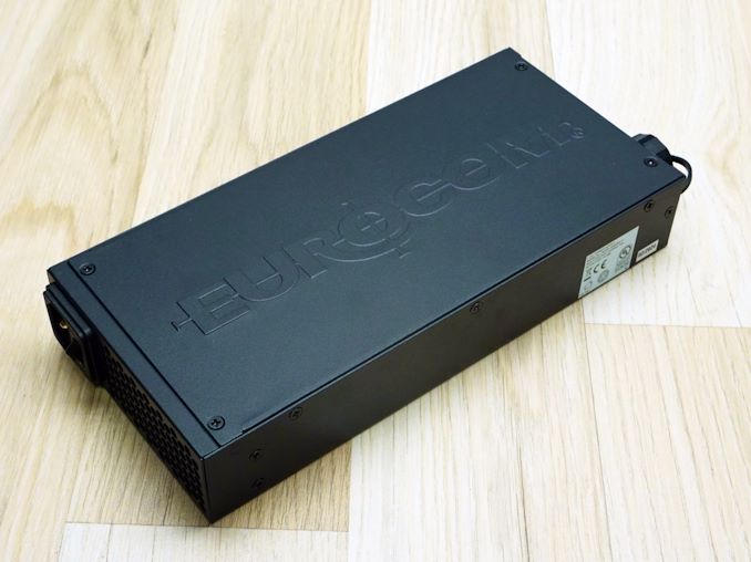
In order to power their own high-end laptops, Eurocom has developed a rather unusual 780W AC adapter for high-performance laptops. Intended to power the most powerful of powerful laptops, their latest power adapter can supply over three-quarters of a kilowatt of DC power; a desktop-like wattage for a desktop-like device. It’s a laptop power adapter that’s unique in its scale, and with some room to scale up even further.
Eurocom 780W AC Adapter Power specifications RAIL +20V MAX OUTPUT 39A 780W DIMENSIONS 325 x 110 x 40mm, 1.38kg AC INPUT 90 - 264 VAC, 50 - 60 Hz MSRP PSU: $299, Cable: $129+Eurocom has offered this adapter for a few years now. But it’s taken on a new life as more laptops have been released that use such a large adapter (or two smaller 300W-ish power adapters). And, critically, Eurocom has made additional DC cable/connector sets for other manufactuers’ laptops, significantly increasing the number of systems it’s compatible with. Currently, Eurocom offers DC cables for the following laptops:
- Alienware M17x M18x; 1x DC Cable ; w/ barrel AW connector; 193cm/6.4ft
- Alienware AREA 51m; 1x DC Cable + Splitter Box w/ 2x barrel AW connectors; 152cm/5ft
- ASUS ROG G18 Strix; GX501V; GM501; GM501GM; GX531GM; 1x DC Cable; w/ barrel ROG connector
- ASUS G703GX, GZ700GX; 1x DC Cable w/ 2x ROG barrel connectors; 152cm/5ft
- CLEVO, OriginPC, Sager, XMG, EUROCOM laptops; 1x DC Cable; w/ 4-pin round connector; 182cm / 6ft
- CLEVO X370SNx; 1x DC Cable; w/ square connector; 120cm / 3.8ft
- CLEVO X170SM/X170KM; 1x DC Cable; w/ dual square connectors; 152cm / 5ft
- Dell Precision 7720/7710; 1x DC Cable; w/ barrel Dell connector; 120cm / 3.8ft
- MSI GE76, GT76, GT77, GE78HX Raider, Titan 18HX 1x DC Cable; w/ single square connector; 120cm / 3.8ft
- MSI laptops & MSI Trident AS Gaming Desktops; 1x DC Cable; w/ 4-pin round connector; 182cm / 6ft
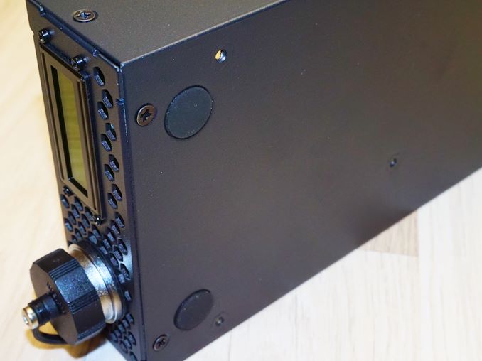
Externally, the Eurocom 780W AC adapter looks like a hybrid between a PC PSU and a laptop adapter. It is shaped like an oversized laptop AC adapter but has a metallic body and cooling vents/fans. Eurocom advertises that it weighs “only 1.34kg”, which is the weight of an entire 14-inch laptop by comparison, but is relatively lightweight for a PSU with that kind of power output. The company logo is debossed across the top side of the adapter, with four round anti-slip pads found at its bottom. Care needs to be taken while moving it around because the metallic edges and weight can spell trouble for wooden surfaces.
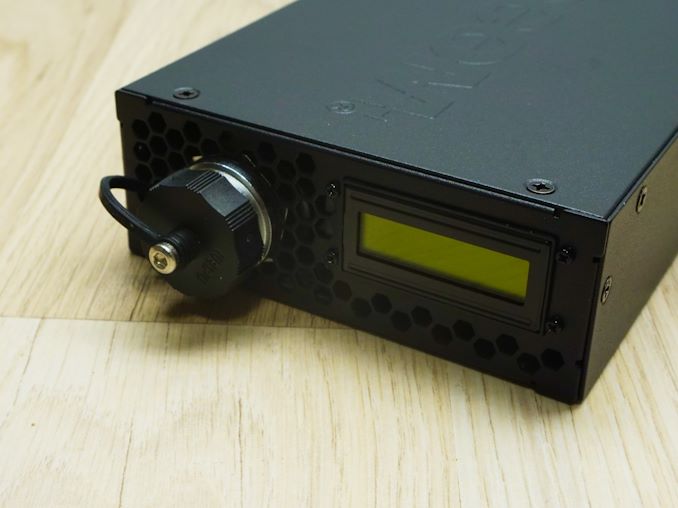
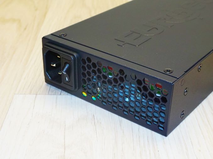
Eurocom installed a small information display on the AC adapter, which shows the current, voltage, and power output, as well as the temperature of the adapter. It is not perfectly accurate – we can see it was reading a 12W load without a DC cable attached to the adapter – but it works as a basic reference. Next to it, there is a heavy-duty metallic connector for the DC cable. On the other side we can find a typical three-prong C14 AC cable receptacle, as well as an on/off switch, which is not something commonly found on laptop AC adapters.
Opening up the chassis, we can see that the Eurocom 780W AC adapter is not unlike common PC PSUs – just less complex due to the need to only generate a single 20V rail. The basic layout is identical, with an AC filter at the input consisting of four Y capacitors, two X capacitors, and two substantial filtering inductors, that leads to a rectifying bridge. The GBJ1508 bridge is made by HY Electronic Cayman Ltd, a Taiwanese company we're encountering for the first time.
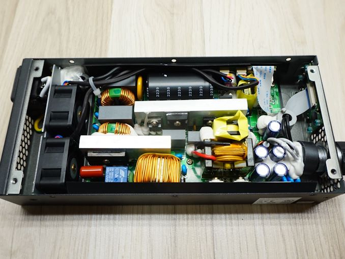
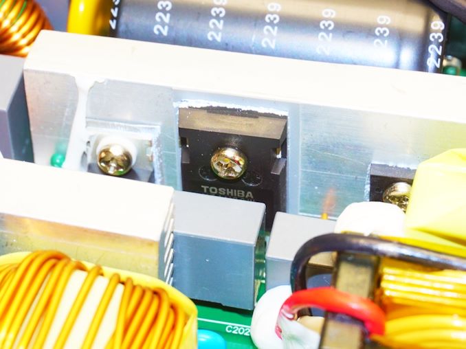
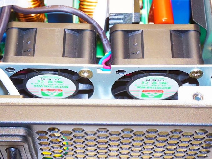
Then we have an APFC circuitry with a massive Aishi 450V/560μF capacitor and a large filtering coil being its passive components, with a Toshiba K31N60W regulator on the same heatsink as the two MOSFETs that form a typical half-bridge configuration. Following that we have a small transformer and two Infineon 045N10N MOSFETs to generate the 20V power output. Cooling is provided by two Protechnic Electric MGT3812XB-W20 38 mm fans, which are small but high quality products with a double-ball bearing engine.
Test Results (~25°C Ambient)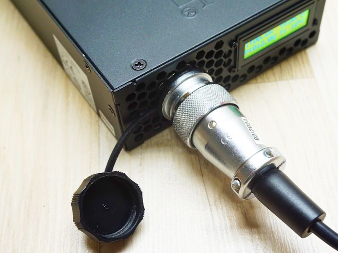
For the testing of PSUs, we are using high precision electronic loads with a maximum power draw of 2700 Watts, a Rigol DS5042M 40 MHz oscilloscope, an Extech 380803 power analyzer, two high precision UNI-T UT-325 digital thermometers, an Extech HD600 SPL meter, and various other bits and parts.
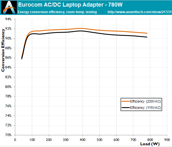
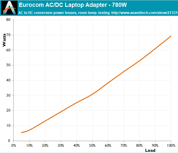
The average efficiency of the Eurocom 780W AC adapter is very high, at 91.6% when the PSU is powered from an 230V AC source and drops down to 90.9% when powered from an 115V AC source. There is no 80Plus or similar efficiency certification covering this PSU, but there is legislation such as the Ecodesign 2019/1782 directive, and, even though the manufacturer does not fully publish its performance specs as the directive requires, the Eurocom 780W adapter seems to easily meet them. We must mention that this kind of PSU has an advantage over classic PC PSUs because it only generates a single voltage line, and conversion losses are lower, so it should not be directly compared to any multi-voltage output PSU.
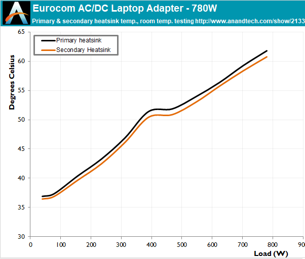
The two small fans of the Eurocom 780W AC adapter seem hardwired to the power output of the unit, largely ignoring the temperature of the adapter and adjusting their speed only according to the load. Up to 40% load, which should cover the power needs of most gaming laptops anyway, the adapter is practically entirely silent. The speed of the fan gradually increases when the load is greater than 330 Watts, reaching terrifying noise figures at maximum load. Given the nature of the adapter, it is highly unlikely that it will operate at such high a load for prolonged periods of time, as even the laptops that require 2x330 Watt adapters will not continuously sustain such a high load.
Power Supply Quality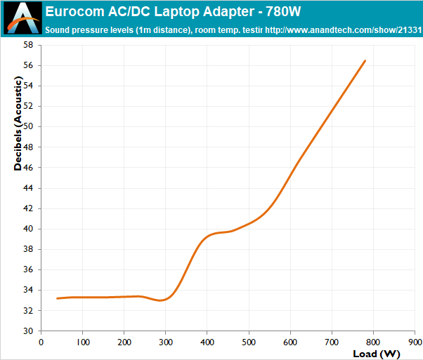
The electrical performance of the Eurocom 780W AC adapter is surprisingly good compared to its datasheet specifications. Eurocom claims a maximum voltage ripple of 200 mV but we recorded a maximum of 116 mV, which is alright for a 20 V rail and better than we expected due to the mediocre secondary side filtering. Voltage regulation is very good, at just 1.2% across the nominal load range.
Main Output Load (Watts) 158.03 394.68 586.46 780.78 Load (Percent) 20% Load 50% Load 75% Load 100% Load Amperes Volts Amperes Volts Amperes Volts Amperes Volts 20 V 7.8 20.26 19.5 20.24 29.25 20.05 39 20.02Line Regulation (20% to 100% load) Voltage Ripple (mV) 20% Load 50% Load 75% Load 100% Load 20V 1.2% 44 66 82 116
During our routine evaluation, we examine the fundamental protection features of all power supply units we review, including Over Current Protection (OCP), Over Voltage Protection (OVP), Over Power Protection (OPP), and Short Circuit Protection (SCP). The Eurocom 780W AC adapter behaves quite oddly here, as it has a rated output of 39 A and a maximum output of 45 A for 25 ms. However, we were able to draw 50 A from the unit, which is nearly 1000 Watts, for several minutes without triggering the OCP/OPP protection. The PSU did not show any serious signs of stress or overheating over that time, nor poor electrical performance. The OPP protection triggers immediately once the load is greater than 50.3 A – and also immediately resets and restarts the PSU when the load drops below 50.2A. It would seem that this platform was initially designed to be significantly more powerful and the OEM “forgot” to adjust the OCP/OPP trigger points.
Conclusion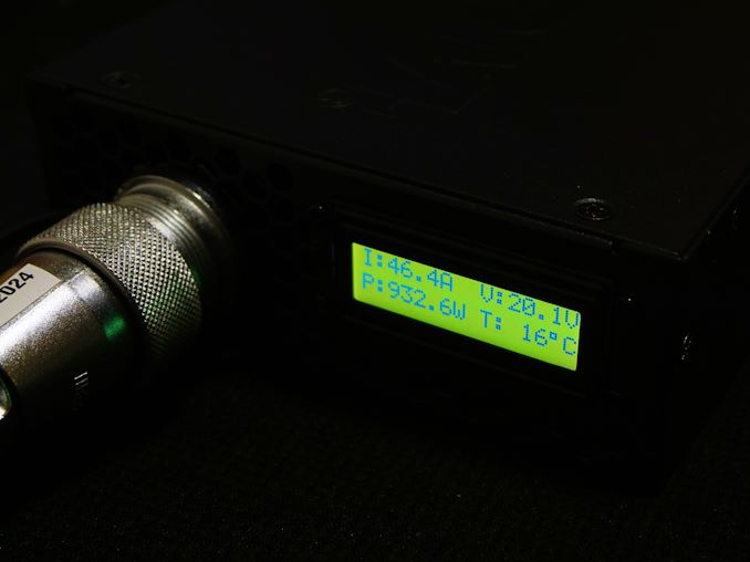
The Eurocom 780W AC adapter melds raw power with innovation, presenting a piece that's as formidable as it is intriguing. With its substantial weight and metallic edges, it demands respect and caution, especially on delicate surfaces. However, its weight is justified by the impressive power output it delivers, making it a powerhouse that somewhat overshadows its bulky, heavy-set design. The inclusion of a display for monitoring performance is a smart touch, though its accuracy leaves room for improvement.
On the inside, Eurocom doesn't skimp on quality. The adapter's internals are a testament to careful selection and engineering, closely mirroring the complexity and efficiency of high-end PC PSUs. Its cooling system, though compact, functions well and provides good performance without compromising on noise levels — at least under most loads. That said, the adapter's noise profile at maximum load might not be everyone's cup of tea, hinting at a balance yet to be perfected between power and tranquility.
Overall, Eurocom's 780W AC adapter boasts commendable efficiency and electrical performance. But as a premium-priced product – a complete unit and cable will set you back at least $429 – it could benefit from a touch more finesse, particularly in terms of user safety and operational noise at high loads. Otherwise, I'm personally a bit surprised that Eurocom isn't offering a open-ended cable for DIY enthusiasts, which could broaden its appeal and utility. Such an addition would not only cater to a wider audience but also underscore Eurocom's commitment to versatility and innovation.
In sum, while the adapter stands out for its power and performance, there's also a clear avenue for Eurocom to enhance its appeal through minor, yet impactful, improvements.
JEDEC Extends DDR5 Memory Specification to 8800 MT/s, Adds Anti-Rowhammer Features
Published: Apr 22nd 2024 8:00am on AnandTech
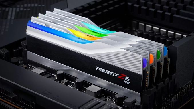
When JEDEC released its DDR5 specification (JESD79) back in 2020, the standard setting organization defined precise specs for modules with speed bins of up to 6400 MT/s, while leaving the spec open to further expansions with faster memory as technology progressed. Now, a bit more than three-and-a-half years later, and the standards body and its members are gearing up to release a faster generation of DDR5 memory, which is being laid out in the newly updated JESD79-JC5 specification. The latest iteration of the DDR5 spec defines official DDR timing specifications up to 8800 MT/s, as well as adding some new features when it comes to security.
Diving in, the new specification outlines settings for memory chips (on all types of memory modules) with data transfer rates up to 8800 MT/s (AKA DDR5-8800). This suggests that all members of the JESD79 committee that sets the specs for DDR5 — including memory chip makers and memory controller designers — agree that DDR5-8800 is a viable extension of the DDR5 specification both from performance and cost point of view. Meanwhile, the addition of higher speed bins is perhaps enabled by another JEDEC feature introduced in this latest specification, which is the Self-Refresh Exit Clock Sync for I/O training optimization.
JEDEC DDR5-A Specifications AnandTech Data Rate MT/s CAS Latency (cycles) Absolute Latency (ns) Peak BW GB/s DDR5-3200 A 3200 22 22 22 13.75 25.6 DDR5-3600 A 3600 26 26 26 14.44 28.8 DDR5-4000 A 4000 28 28 28 14 32 DDR5-4400 A 4400 32 32 32 14.55 35.2 DDR5-4800 A 4800 34 34 34 14.17 38.4 DDR5-5200 A 5200 38 38 38 14.62 41.6 DDR5-5600 A 5600 40 40 40 14.29 44.8 DDR5-6000 A 6000 42 42 42 14 48 DDR5-6400 A 6400 46 46 46 14.38 51.2 DDR5-6800 A 6800 48 48 48 14.12 54.4 DDR5-7200 A 7200 52 52 52 14.44 57.6 DDR5-7600 A 7600 54 54 54 14.21 60.8 DDR5-8000 A 8000 56 56 56 14 64.0 DDR5-8400 A 8400 60 60 60 14.29 67.2 DDR5-8800 A 8800 62 62 62 14.09 70.4When it comes to the JEDEC standard for DDR5-8800, it sets relatively loose timings of CL62 62-62 for A-grade devices and CL78 77-77 for lower-end C-grade ICs. Unfortunately, the laws of physics driving DRAM cells have not improved much over the last couple of years (or decades, for that matter), so memory chips still must operate with similar absolute latencies, driving up the relative CAS latency. In this case 14ns remains the gold standard, with CAS latencies at the new speeds being set to hold absolute latencies around that mark. But in exchange for systems willing to wait a bit longer (in terms of cycles) for a result, the new spec improves the standard's peak memory bandwidth by 37.5%.
This of course is just the timings set in the JEDEC specification, which is primarily of concern for server vendors. So we'll have to see just how much harder consumer memory manufacturers can push things for their XMP/EXPO-profiled memory. Extreme overclockers are already hitting speeds as high as 11,240 MT/s with current-generation DRAM chips and CPUs, so there may be some more headroom to play with in the next generation.
Meanwhile, on the security front, the updated spec makes a couple of changes that have been put in place seemingly to address rowhammer-style exploits. The big item here is Per-Row Activation Counting (PRAC), which true to its name, enables DDR5 to keep a count of how often a row has been activated. Using this information, memory controllers can then determine if a memory row has been excessively activated and is at risk of having its bits flipped, at which point they can back off to let the row properly refresh and the data re-stabilize.
Notably here, the JEDEC press release doesn't use the rowhammer name at any point (unfortunately, we haven't been able to see the specification itself). But based on the description alone, this is clearly intended to thwart rowhammer attacks, since these normally operate by forcing a bit flip between refreshes through a large number of activations.
Digging a bit deeper, PRAC seems to be based on a recent Intel patent, Perfect Row Hammer Tracking with Multiple Count Increments (US20220121398A1), which describes a very similar mechanism under the name "Perfect row hammer tracking" (PRHT). Notably, the Intel paper calls out that this technique has a performance cost associated with it because it increases the overall row cycle time. Ultimately, as the vulnerability underpinning rowhammer is a matter of physics (cell density) rather than logic, it's not too surprising to see that any mitigation of it comes with a cost.
The updated DDR5 specification also depreciates support for Partial Array Self Refresh (PASR) within the standard, citing security concerns. PASR is primarily aimed at power efficiency for mobile memory to begin with, and as a refresh-related technology, presumably overlaps some with rowhammer – be it a means to attack memory, or an obstruction to defending against rowhammer. Either way, with mobile devices increasingly moving to low-power optimized LPDDR technologies anyhow, the depreciation of PASR does not immediately look like a major concern for consumer devices.
SK Hynix and TSMC Team Up for HBM4 Development
Published: Apr 19nd 2024 11:00am on AnandTech
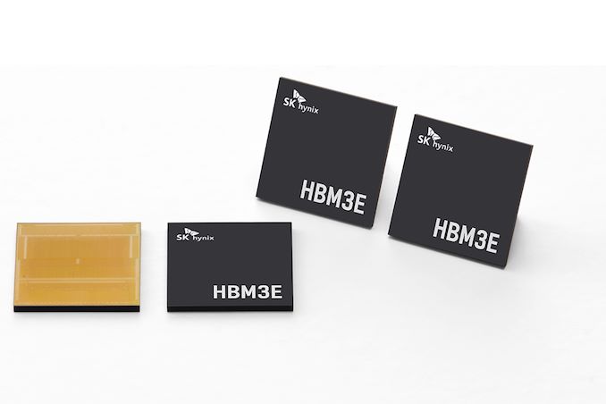
SK hynix and TSMC announced early on Friday that they had signed a memorandum of understanding to collaborate on developing the next-generation HBM4 memory and advanced packaging technology. The initiative is designed to speed up the adoption of HBM4 memory and solidify SK hynix's and TSMC's leading positions in high-bandwidth memory and advanced processor applications.
The primary focus of SK hynix's and TSMC's initial efforts will be to enhance the performance of the HBM4 stack's base die, which (if we put it very simply) acts like an ultra-wide interface between memory devices and host processors. With HBM4, SK hynix plans to use one of TSMC's advanced logic process technologies to build base dies to pack additional features and I/O pins within the confines of existing spatial constraints.
This collaborative approach also enables SK hynix to customize HBM solutions to satisfy diverse customer performance and energy efficiency requirements. HBM has been touting custom HBM solutions for a while, and teaming up with TSMC will undoubtedly help with this.
"TSMC and SK hynix have already established a strong partnership over the years. We've worked together in integrating the most advanced logic and state-of-the art HBM in providing the world's leading AI solutions," said Dr. Kevin Zhang, Senior Vice President of TSMC's Business Development and Overseas Operations Office, and Deputy Co-Chief Operating Officer. "Looking ahead to the next-generation HBM4, we're confident that we will continue to work closely in delivering the best-integrated solutions to unlock new AI innovations for our common customers."
Furthermore, the collaboration extends to optimizing the integration of SK hynix's HBM with TSMC's CoWoS advanced packaging technology. CoWoS is among the most popular specialized 2.5D packaging process technologies for integrating logic chips and stacked HBM into a unified module.
For now, it is expected that HBM4 memory will be integrated with logic processors using direct bonding. However, some of TSMC's customers might prefer to use an ultra-advanced version of CoWoS to integrate HBM4 with their processors.
"We expect a strong partnership with TSMC to help accelerate our efforts for open collaboration with our customers and develop the industry's best-performing HBM4," said Justin Kim, President and the Head of AI Infra at SK hynix. "With this cooperation in place, we will strengthen our market leadership as the total AI memory provider further by beefing up competitiveness in the space of the custom memory platform."