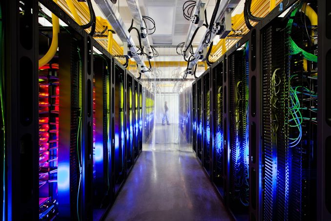
SK hynix Reports That 2025 HBM Memory Supply Has Nearly Sold Out
Published: May 2nd 2024 11:00am on AnandTech
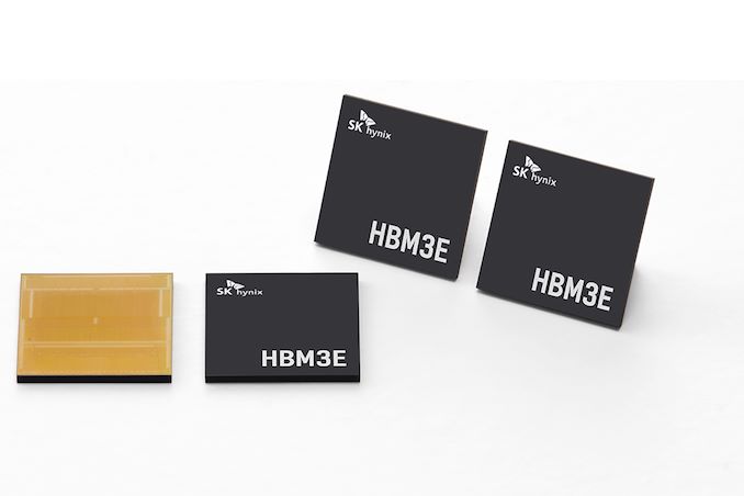
Demand for high-performance processors for AI training is skyrocketing, and consequently so is the demand for the components that go into these processors. So much so that SK hynix this week is very publicly announcing that the company's high-bandwidth memory (HBM) production capacity has already sold out for the rest of 2024, and even most of 2025 has already sold out as well.
SK hynix currently produces various types of HBM memory for customers like Amazon, AMD, Facebook, Google (Broadcom), Intel, Microsoft, and, of course, NVIDIA. The latter is an especially prolific consumer of HBM3 and HBM3E memory for its H100/H200/GH200 accelerators, as NVIDIA is also working to fill what remains an insatiable (and unmet) demand for its accelerators.
As a result, HBM memory orders, which are already placed months in advance, are now backlogging well into 2025 as chip vendors look to secure supplies of the memory stacks critical to their success.
This has made SK hynix the secnd HBM memory vendor in recent months to announce that they've sold out into 2025, following an earlier announcement from Micron regarding its HBM3E production. But of the two announcements, SK hynix's is arguably the most significant yet, as the South Korean firm's HBM production capacity is far greater than Micron's. So while things were merely "interesting" with the smallest of the Big Three memory manufacturers being sold out into 2025, things are taking a more concerning (and constrained) outlook now that SK hynix is as well.
SK hynix currently controls roughly 46% - 49% of HBM market, and its share is not expected to drop significantly in 2025, according to market tracking firm TrendForce. By contrast, Micron's share on HBM memory market is between 4% and 6%. Since HBM supply of both companies is sold out through the most of 2025, we're likely looking at a scenario where over 50% of the industry's total HBM3/HBM3E supply for the coming quarters is already sold out.
This leaves Samsung as the only member of the group not to comment on HBM demand so far. Though with memory being a highly fungible commodity product, it would be surprising if Samsung wasn't facing similar demand. And, ultimately, all of this is pointing towards the indusry entering an HBM3 memory shortage.
Separately, SK hynix said that it is sampling 12-Hi 36GB HBM3E stacks with customers and will begin volume shipments in the third quarter.
The XPG Core Reactor II VE 850W PSU Review: Our First ATX 3.1 Power Supply
Published: May 2nd 2024 10:00am on AnandTech
Just over 18 months ago, Intel launched their significantly revised ATX v3.0 power supply standard, and with it, the 600 Watt-capable 12VHPWR cable to power video cards and other high-drain add-in cards. The release of the standard came with a lot of fanfare and excitement – the industry was preparing for a future where even flagship video cards could go back to being powered by a single cable – but shortly after, things became exciting again for all the wrong reasons.
The new 12VHPWR connector proved to be less forgiving of poor connections between cables and devices than envisioned. With hundreds of watts flowing through the relatively small pins – and critically, insufficient means to detect a poor connection – a bad connection could result in a thermal runaway scenario, i.e. a melted connector. And while the issue was an edge case overall, affecting a fraction of a fraction of systems, even a fraction is too much when you're starting from millions of PCs, never mind the unhappy customers with broken video cards.
So the PC industry is taking a mulligan on the matter, quickly revising the ATX specification and the 12VHPWR connector to fix their design flaws. In its place we have the new ATX v.3.1 power supply specification, as well as the associated 12V-2×6 connector, the combination of which are intended to serve the same goals, but with far less of a chance of errant electricity causing damage.
Ultimately, the combination of the two new standards has required backwards-compatible changes on both the device (video card) side, as well as the power supply side. And as a result, power supply manufacturers are now in the process of releasing ATX v3.1-compliant PSUs that implement these revisions. For PSU vendors, the changes are relatively trivial overall, but they are none the less important changes that for multiple reasons, they are making sure to promote.
Getting down to business, the first ATX v3.1 power supply to enter our testing labs comes from ADATA sub-brand XPG, a prolific player in the PSU market. XPG recently expanded its product lineup with the introduction of the Core Reactor II VE series, the company's first foray into ATX 3.1-compliant PSUs. As a direct successor of the Core Reactor II series, the Core Reactor II VE is a relatively simple 80Plus Gold unit that distinguishes itself with its straightforward design, aimed at providing steady performance without the high expense.
In today’s review, we are taking a look at the 850W version of the Core Reactor II VE series, which is, for the time being, the most powerful ATX 3.1 unit XPG offers.
AMD Zen 5 Status Report: EPYC "Turin" Is Sampling, Silicon Looking Great
Published: May 1nd 2024 6:00am on AnandTech
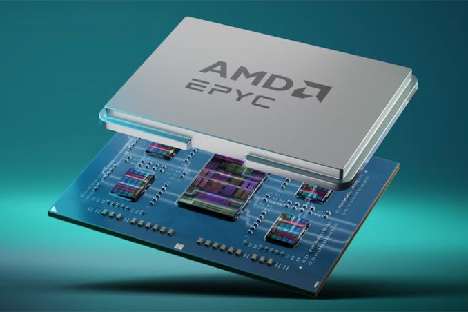
As part of AMD's Q1'2024 earnings announcement this week, the company is offering a brief status update on some of their future products set to launch later this year. Most important among these is an update on their Zen 5 CPU architecture, which is expected to launch for both client and server products later this year.
Highlighting their progress so far, AMD is confirming that EPYC "Turin" processors have begun sampling, and that these early runs of AMD's next-gen datacenter chips are meeting the company's expectations.
"Looking ahead, we are very excited about our next-gen Turin family of EPYC processors featuring our Zen 5 core," said Lisa Su, chief executive officer of AMD, at the conference call with analysts and investors (via SeekingAlpha). "We are widely sampling Turin, and the silicon is looking great. In the cloud, the significant performance and efficiency increases of Turin position us well to capture an even larger share of both first and third-party workloads."
Overall, it looks like AMD is on-track to solidify its position, and perhaps even increase its datacenter market share with its EPYC Turin processors. According to AMD, the company's server partners are developing a 30% larger number of designs for Turin than they did Genoa. This underscores how AMD's partners are preparing for even more market share growth on the back of AMD's ongoing success, not to mention the improved performance and power efficiency that the Zen 5 architecture should offer.
"In addition, there are 30% more Turin platforms in development from our server partners, compared to 4th Generation EPYC platforms, increasing our enterprise and with new solutions optimized for additional workloads," Su said. "Turin remains on track to launch later this year."
AMD's EPYC 'Turin' processors will be drop-in compatible with existing SP5 platforms (i.e., will come in an LGA 6096 package), which will facilitate its faster ramp and adoption of the platform both by cloud giants and server makers. In addition, AMD's next-generation EPYC CPUs are expected to feature more than 96 cores and a more versatile memory subsystem.
PCI-SIG Completes CopprLink Cabling Standard: PCIe 5.0 & 6.0 Get Wired
Published: May 1nd 2024 10:00am on AnandTech
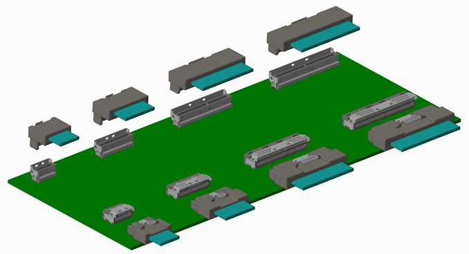
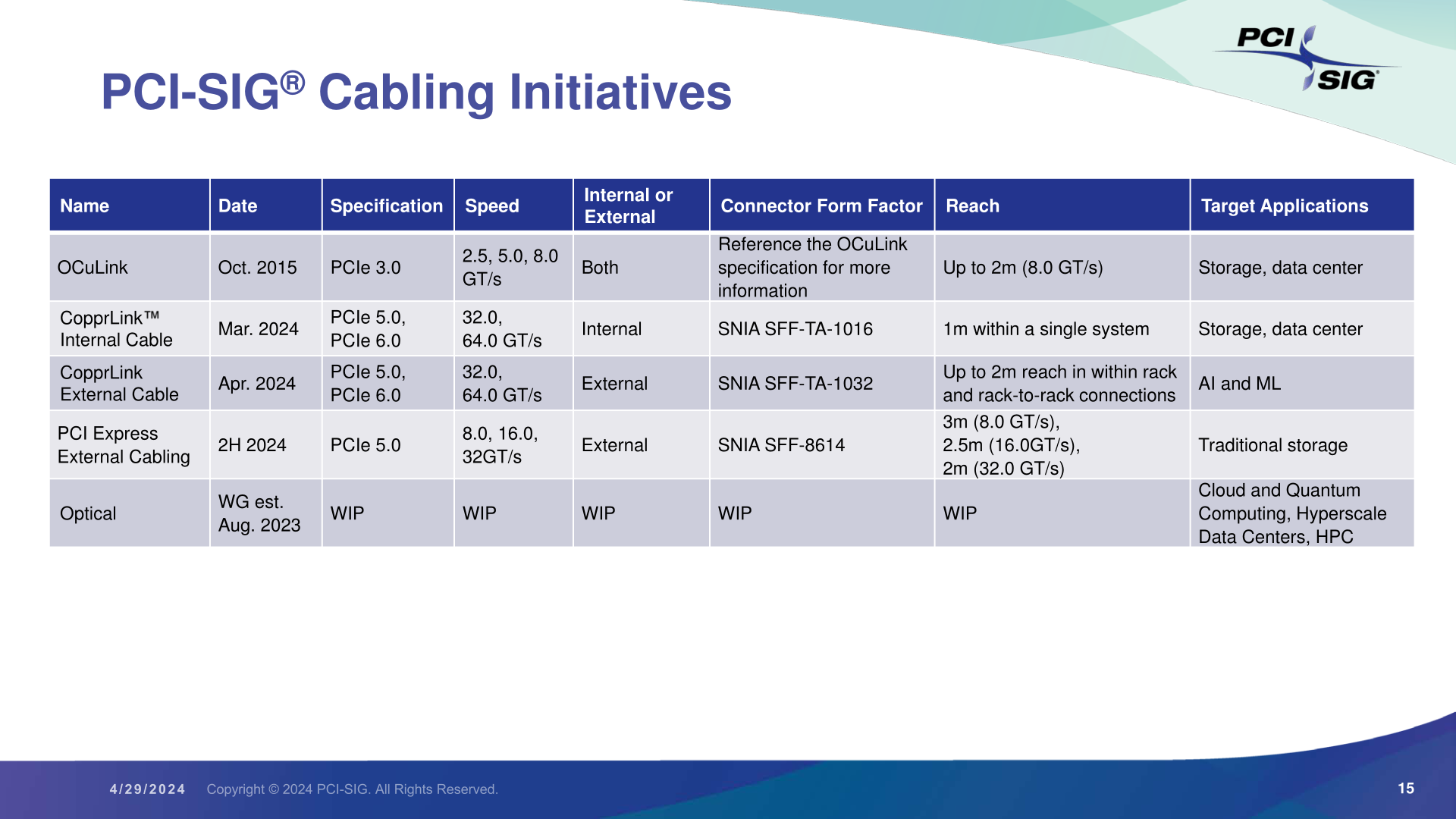
The PCI-SIG sends word over this morning that the special interest group has completed their development efforts on the group’s new PCI-Express cabling standard, CopprLink. Designed to go hand-in-hand with PCIe 5.0 and PCIe 6.0, CopprLink defines both internal and external copper cabling for the latest PCIe standards, giving system vendors and assemblers the ability to use wires to connect devices within a system, or even whole systems.
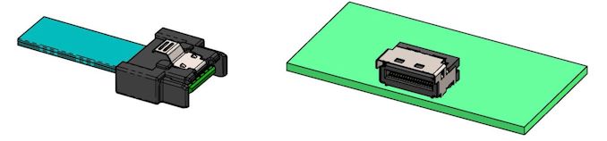
The CopprLink standard is, in practice, a pair of standards sharing the same brand-name under the PCI-SIG umbrella. The internal standard, “CopprLink Internal Cable”, is designed to allow for a new generation of PCIe cables up to 1 meter in length that are capable of sustaining PCIe 5.0 and PCIe 6.0 signaling. Internal CopprLink effectively supplants a host of older internal PCIe cabling standards (including the abandoned OCuLink), which were originally designed for earlier generations of PCIe signaling.
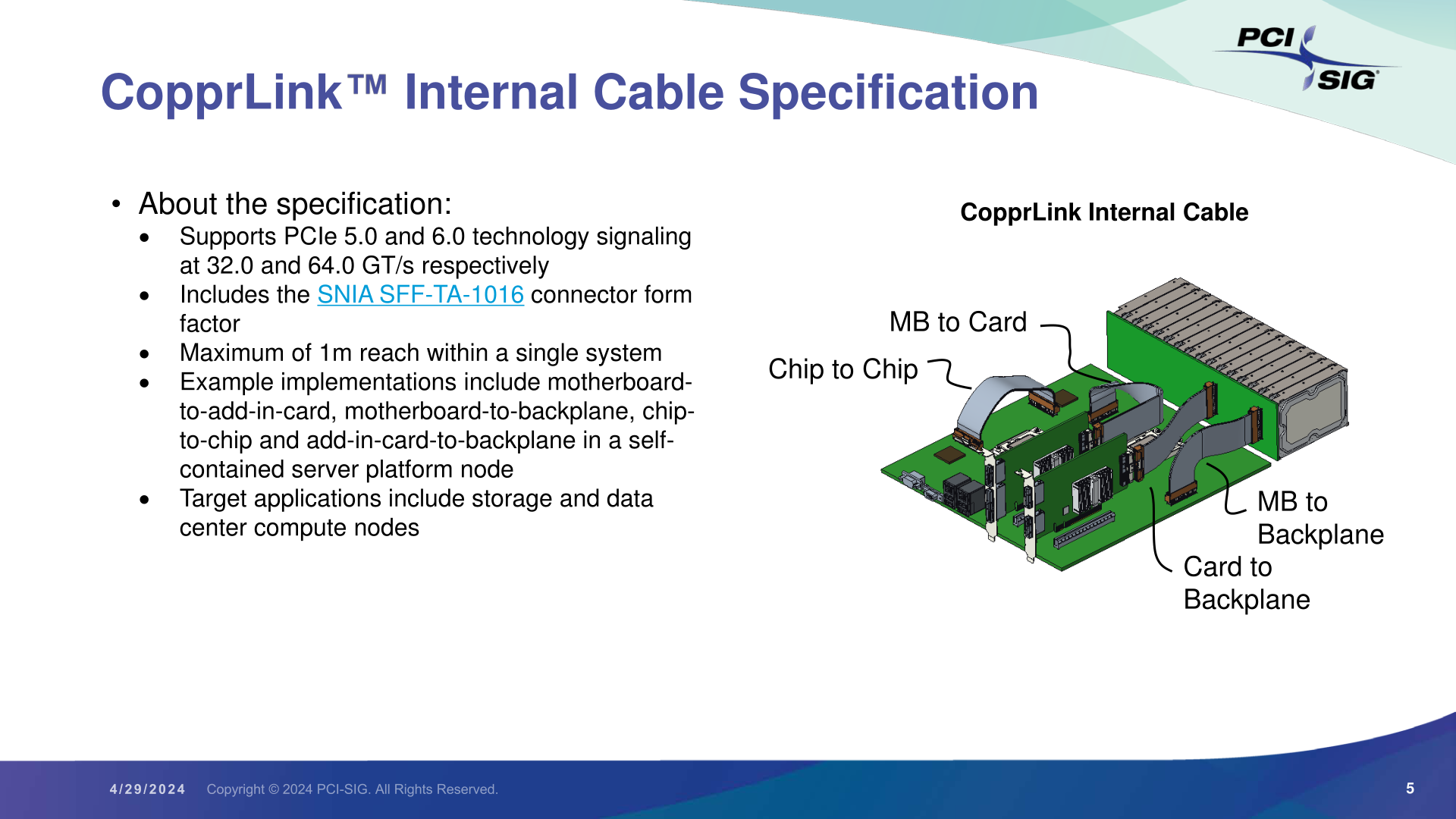
At a high level, internal CopprLink is intended to provide not only host-to-device connectivity, but even more transparent backhaul applications such as motherboard-to-backplane connectivity, and unique applications such as chip-to-chip PCIe connections. In other words, CopprLink allows for cabled PCIe to be used in almost any situation where a PCIe connection needs to be established within a system. Strictly speaking, CopprLink doesn't replace the PCIe CEM connector in any way – but the relatively thick copper cables have less signal loss than PCB traces, making a cabled standard extremely useful even for internal connections. PCI-SIG sees CopprLink cables taking hold in the storage and data center markets, product categories where we already see PCIe cabling in use today.
The companion connector standard for internal CopprLink is the SNIA-developed SFF-TA-1016 connector, which bears more than a passing resemblance to the widely-used SFF-8654 (SlimSAS) connector. SFF-TA-1016 is available in x4, x8, and x16 configurations, and while the PCI-SIG doesn’t go so far as to defining widths within their own standard, the connectors available paint a clear picture of the options at hand. Internal CopprLink x4 should be especially popular with storage, as we already see today.
 Top: SFF-TA-1016 Family of Connectors (Figure 4-1, Image Courtesy SNIA)
Bottom: Sample SFF-TA-1016 x4 Contact Plug and Recepticle (Figure 4-2, Image Courtesy SNIA)
Top: SFF-TA-1016 Family of Connectors (Figure 4-1, Image Courtesy SNIA)
Bottom: Sample SFF-TA-1016 x4 Contact Plug and Recepticle (Figure 4-2, Image Courtesy SNIA)
Meanwhile, the group has also developed an external cabling standard to cover those same PCIe 5.0/6.0 data rates. External CopprLink cables can go up to 2 meters, allowing for board-to-board connections within a rack, and even short rack-to-rack PCIe connections.
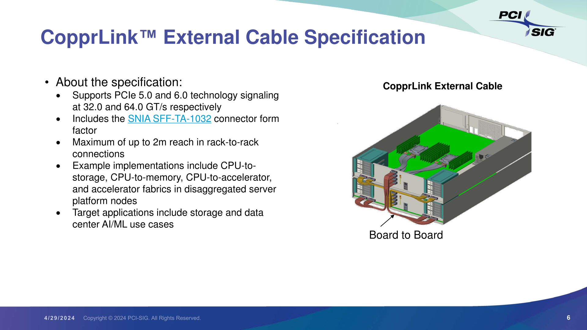
The external version of CopprLink also uses a more robust connector, relying on SNIA’s SFF-TA-1032 standard. Like internal/1016, this is available with x4, x8, and x16 configurations, using 44, 68, and 120 positions/pins respectively. The PCI-SIG is expecting this version of the standard to be primarily adopted by the AI/Machine Learning markets, which need to move heaps of data between systems. Notably, however, they don’t really expect the storage market to make use of this spec – instead, they’ll be served by an updated version of the classic PCI Express External Cabling standard.
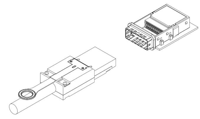 SFF-TA-1032 x16 Plug and Connector (Figure 4-1, Image Courtesy SNIA)
Finally, a bit farther out on the group’s roadmap, PIG-SIG is also reiterating that they’re working on a new optical cabling standard as well. The workgroup for this project was established in 2023, so the project is still in its early days. Notably, the forthcoming optical standard is intended to be optical technology-agnostic, allowing for PCIe to be paired with a variety of optical technologies.
In the meantime, with the internal and external CopprLink standards completed, the PCI-SIG is hoping to quickly move this cabling into production. Since these are solely cabling standards – and thus don’t require intensive development efforts such as new controllers or the like – the group is hoping that their members will have something to show off in time for the group’s developer conference this summer, or the Flash Memory Summit in August. After which, hardware vendors should be able to deploy the new cables relatively quickly.
Gallery: PCI-SIG CopprLink Press Deck


Samsung Foundry Update: 2nm Unveil in June, Second-Gen SF3 3nm Hits Production This Year
Published: May 1nd 2024 8:00am on AnandTech
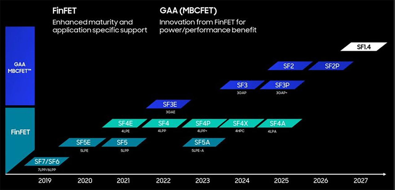
As part of Samsung's Q1 earnings announcement, the company has outlined some of its foundry unit's key plans for the rest of the year. The company has confirmed that it remains on track to meeting its goal of starting mass production of chips on its SF3 (3 nm-class, 2nd Generation) technology in the second half of the year. Meanwhile in June, Samsung Foundry will formally unveil its SF2 (2 nm-class) process technology, which will offer a mix of performance and efficiency enhancements. Finally, the company the company is preparing a variation of its 4 nm-class technology for integration into stacked 3D designs.
SF2 To Be Unveiled In JuneSamsung plans to disclose key details about its SF2 fabrication technology at the VLSI Symposium 2024 on June 19. This will be the company's second major process node based upon gate-all-around (GAA) multi-bridge channel field-effect transistors (MBCFET). Improving over its predecessor, SF2 will feature a 'unique epitaxial and integration process,' which will give the process node higher performance and lower leakage than traditional FinFET-based nodes (though Samsung isn't disclosing the specific node they're comparing it to).
Samsung says that SF2 increases performance of narrow transistors by 29% for N-type and 46% for P-type, and wide transistors by 11% and 23% respectively. Moreover, it reduces transistor global variation by 26% compared to FinFET technology, and cuts product leakage by approximately 50%. This process also sets the stage for future advancements in technology through enhanced design technology co-optimization (DTCO) collaboration with its customers.
One thing that Samsung has not mentioned in context of SF2 is backside power delivery, so at least for the moment, there is no indication that Samsung will be adopting this next-gen power routing feature for SF2.
Samsung says that the design infrastructure for SF2 – the PDK, EDA tools, and licensed IP – will be finalized in the second quarter of 2024. Once this happens, Samsung's chip development partners will be able to begin designing products for this production node. Meanwhile, Samsung is already working with Arm to co-optimize Arm's Cortex cores for the SF2 process.
SF3: On Track for 2H 2024As the first fab to introduce a GAAFET-based node, Samsung has been on the cutting edge of chip construction. At the same time, however, that has also meant that they're the first fab to encounter and solve the inevitable teething issues that come with such a major transistor design change. Consequently, while Samsung's first-generation SF3E process technology has been in production for a little less than two years now, the only publicly-disclosed chips made on the process so far have been relatively small cryptocurrency mining chips – exactly the kind of pipecleaner parts that do well on a new process node.
But with that experience in hand, Samsung is preparing to move on to making bigger and better chips with GAAFETs. As part of their earnings announcements, the company has confirmed that their updated SF3 node, which was introduced last year, remains on schedule to enter production in the second half of 2024.
A more mature product from the get-go, SF3 is being prepared to be used for building larger processors, including datacenter products. Compared to its direct predecessor, SF4, SF3 promises a 22% performance boost at the same power and transistor count, or a 34% lower power at the same frequency and complexity, as well as a 21% logic area reduction. In general, Samsung pins a lot of hopes on this technology, as it's this generation of their 3nm-class technology that is poised to compete against TSMC's N3B and N3E nodes.
SF4: Ready for 3D StackingFinally, Samsung is also preparing a variant of their final FinFET technology node, SF4, for use in 3D chiplet stacking. As transistor density improvements have continued to slow, 3D chip stacking has emerged as a way to keep boosting overall chip performance, especially with modern, multi-tile processor designs.
Details on this node are limited, but it would seem that Samsung is making some changes to account/optimize for using SF4-fabbed chiplets in a 3D-stacked design, where chips need to be able to communicate both up and down. According to the company's Q1 financial report, Samsung expects to complete their preparatory work on the chip-stacking SF4 variant during the current quarter (Q2).
TSMC Readies 8x Reticle Super Carrier Interposer For Next-Gen Chips Twice as Large As Today's
Published: Apr 30nd 2024 9:00am on AnandTech
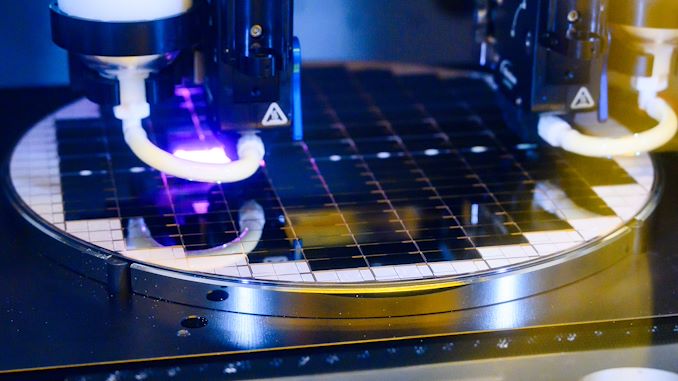
TSMC is no stranger to building big chips. Besides the ~800mm2 reticle limit of their normal logic processes, the company already produces even larger chips by fitting multiple dies on to a single silicon interposer, using their chip-on-wafer-on-substrate (CoWoS) technology. But even with current-gen CoWoS allowing for interposers up to 3.3x TSMC's reticle limit, TSMC plans to build bigger still in response to projected demand from the HPC and AI industries. To that end, as part of the company's North American Technology Symposium last week, TSMC announced that they are developing the means of building super-sized interposers that can reach over 8x the reticle limit.
TSMC's current-generation CoWoS technology allows for building interposers up to 2831 mm2 and the company is already seeing customers come in with designs that run up to those limits. Both AMD's Instinct MI300X accelerator and NVIDIA's forthcoming B200 accelerator are prime examples of this, as they pack huge logic chiplets (3D stacked in case of AMD's product) and eight HBM3/HBM3E memory stacks in total. The total space afforded by the interposer gives these processors formidable performance, but chip developers want to go more powerful still. And to get there as quickly as possible, they'll need to go bigger as well in order to incorporate more logic chiplets and more memory stacks.
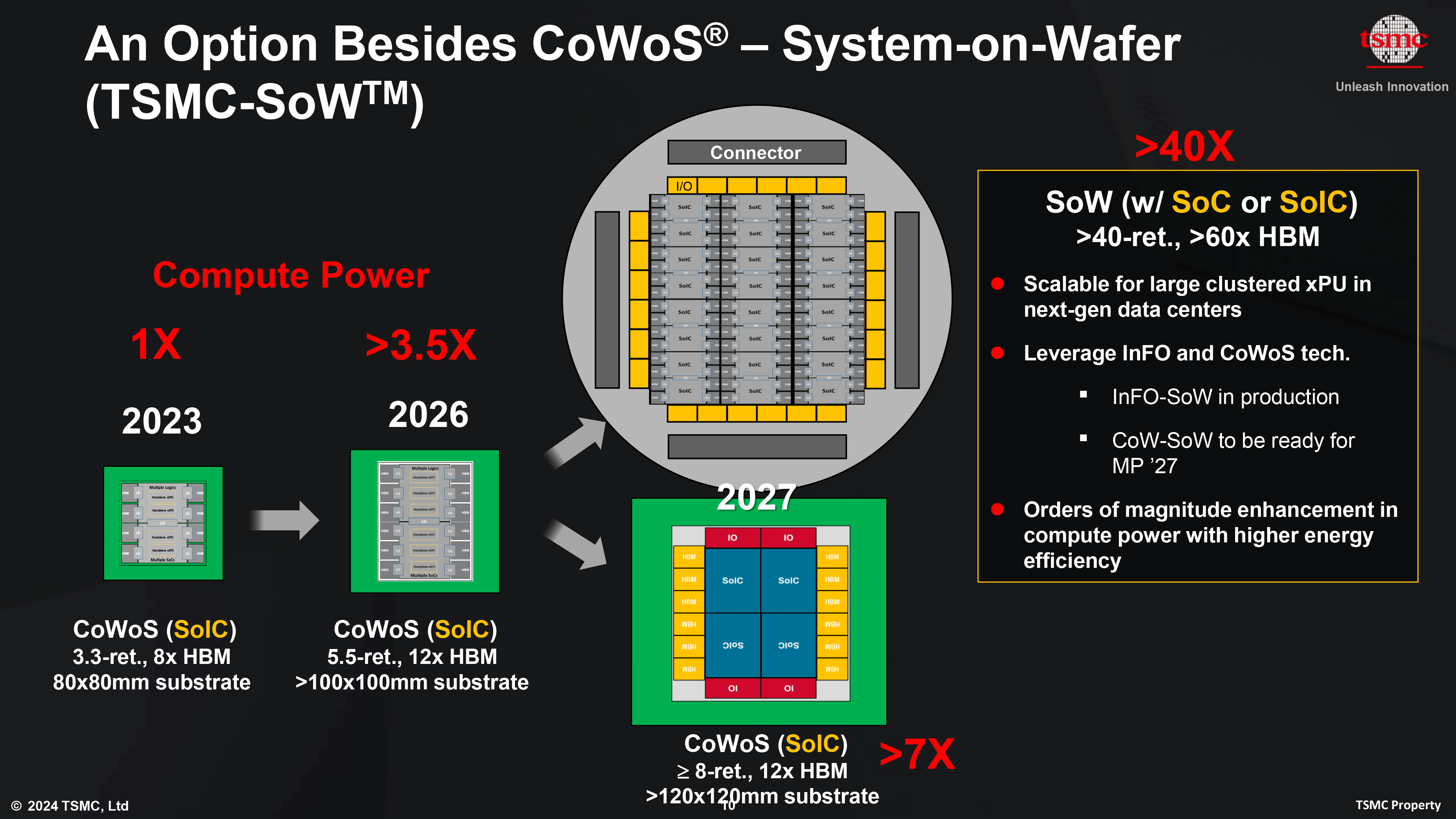
For their next-generation CoWoS product that's set to launch in 2026, TSMC plans to release CoWoS_L, which will offer a maximum interposer size of approximately 5.5 times that of a photomask, totaling 4719 mm² altogether. This next generation package will support up to 12 HBM memory stacks and will necessitate a larger substrate measuring at 100×100 mm. Coupled with process node improvements over the next few years, and TSMC expects chips based on this generation of CoWoS to offer better than 3.5x the compute performance of current-generation CoWoS chips.
Farther down the line, in 2027 TSMC intends introduce a version of CoWoS that allows for interposers up to 8 times larger than the reticle limit. This will offer an ample 6,864 mm² of space for chiplets on a substrate that measures 120×120 mm. TSMC envisions leveraging this technology for designs that integrate four stacked systems-on-integrated chips (SoICs), with 12 HBM4 memory stacks and extra I/O dies. TSMC roughly projects that this will enable chip designers to once again double performance, producing chips that surpass 7x the performance of current-generation chips.
Of course, building such large chips will come with its own set of consequences, above and beyond what TSMC will have to deal with. Enabling chip designers to build such grand processors is going to impact system design, as well as how datacenters accommodate these systems. TSMC's 100×100mm substrate will be riding right up to the limit of the OAM 2.0 form factor, whose modules measure 102×165mm to begin with. And if that generation of CoWoS doesn't break the current OAM form factor, then 120×120mm chips certainly will. And, of course, all of that extra silicon requires additional power and cooling, which is why we're already seeing hardware vendors prepare for how to cool multi-kilowatt chips by investigating liquid and immersion cooling.
Ultimately, even if Moore's Law has slowed to a crawl in terms of delivering transistor density improvements, CoWoS offers an out for producing chips with an ever-larger number of transistors. So with TSMC set to offer interposers and substrates with over twice the area of today's solutions, big chips intended for HPC systems are only going to continue to grow in both performance and size.
Related Reading- TSMC's 1.6nm Technology Announced for Late 2026: A16 with "Super Power Rail" Backside Power
- TSMC 2nm Update: N2 In 2025, N2P Loses Backside Power, and NanoFlex Brings Optimal Cells
- TSMC Preps Cheaper 4nm N4C Process For 2025, Aiming For 8.5% Cost Reduction
- TSMC's System-on-Wafer Platform Goes 3D: CoW-SoW Stacks Up the Chips
- TSMC Jumps Into Silicon Photonics, Lays Out Roadmap For 12.8 Tbps COUPE On-Package Interconnect
In Light of Stability Concerns, Intel Issues Request to Motherboards Vendors to Actually Follow Stock Power Settings
Published: Apr 29nd 2024 9:30am on AnandTech
Across the internet, from online forums such as Reddit to various other tech media outlets, there's a lot of furor around reports of Intel's top-end 14th and 13th Gen K series of processors running into stability issues. As Intel's flagship chips, these parts come aggressively clocked in order to maximize performance through various implementations of boost and turbo, leaving them running close to their limits out of the box. But with high-end motherboards further goosing these chips to wring even more performance out of them, it would seem that the Intel desktop ecosystem has finally reached a tipping point where all of these efforts to boost performance have pushed these flagship chips to unstable conditions. To that end, Intel has released new gudiance to its consumer motherboard partners, strongly encouraging them to actually implment Intel's stock power settings, and to use those baseline settings as their out-of-the-box default.
While the underlying conditions are nothing new – we've published stories time and time again about motherboard features such as multi-core enhancement (MCE) and raised power consumption limits that seek to maximize how hard and how long systems are able to turbo boost – the issue has finally come to a head in the last couple of months thanks to accumulating reports of system instability with Intel's 13900K and 14900K processors. These instability problems are eventually solved by either tamping down on these motherboard performance-boosting features – bringing the chips back down to something closer to Intel's official operating parameters – or downclocking the chips entirely.
Intel first began publicly investigating the matter on the 27th of February, when Intel's Communications Manager, Thomas Hannaford, posted a thread on Intel's Community Product Support Forms titled "Regarding Reports of 13th/14th Gen Unlocked Desktop Users Experiencing Stability Issues". In this thread, Thomas Hannaford said, "Intel is aware of reports regarding Intel Core 13th and 14th Gen unlocked desktop processors experiencing issues with certain workloads. We're engaged with our partners and are conducting analysis of the reported issues. If you are experiencing these issues, please reach out to Intel Customer Support for further assistance in the interim."
Since that post went up, additional reports have been circulating about instability issues across various online forums and message boards. The underlying culprit has been theorized to be motherboards implementing an array of strategies to improve chip performance, including aggressive multi-core enhancement settings, "unlimited" PL2 turbo, and reduced load line calibration settings. At no point do any of these settings overclock a CPU and push it to a higher clockspeed than it's validated for, but these settings do everything possible to keep a chip at the highest clockspeed possible at all times – and in the process seem to have gone a step too far.
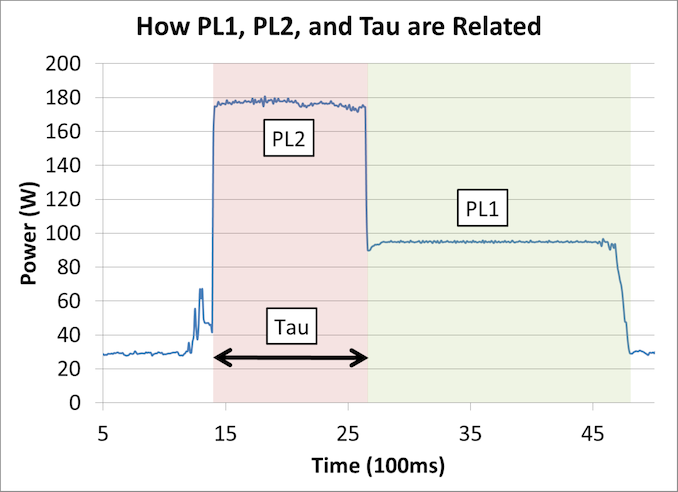 From "Why Intel Processors Draw More Power Than Expected: TDP and Turbo Explained"
We wrote a piece initially covering multi-core enhancement in 2012, detailing how motherboard manufacturers try to stay competitive with each other and leverage any headroom within the silicon to output the highest performance levels. And more recently, we've talked about how desktop systems with Intel chips are now regularly exceeding their rated TDPs – sometimes by extreme amounts – as motherboard vendors continue to push them to run as hard as possible for the best performance.
But things have changed since 2012. At the time, this wasn't so much of an issue, as overclocking was actually very favorable to increasing the performance of processors. But in 2024 with chips such as the Intel Core i9-14900K, we have CPUs shipping with a maximum turbo clock speed of 6.0 GHz and a peak power consumption of over 400 Watts, figures that were only a pipe dream a decade ago.
Jumping to the present time, over the weekend Intel released a statement about the matter to its partners, outlining their investigation so far and their suggestions/requests to their partners. That statement was quickly leaked to the press, with Igorslab.de and others breaking the news. Since then, we've been able to confirm through official sources that this is a real and accurate statement from Intel.
This statement reads as follows:
Intel® has observed that this issue may be related to out of specification operating conditions resulting in sustained high voltage and frequency during periods of elevated heat.
Analysis of affected processors shows some parts experience shifts in minimum operating voltages which may be related to operation outside of Intel® specified operating conditions.
While the root cause has not yet been identified, Intel® has observed the majority of reports of this issue are from users with unlocked/overclock capable motherboards.
Intel® has observed 600/700 Series chipset boards often set BIOS defaults to disable thermal and power delivery safeguards designed to limit processor exposure to sustained periods of high voltage and frequency, for example:
– Disabling Current Excursion Protection (CEP) – Enabling the IccMax Unlimited bit – Disabling Thermal Velocity Boost (TVB) and/or Enhanced Thermal Velocity Boost (eTVB) – Additional settings which may increase the risk of system instability: – Disabling C-states – Using Windows Ultimate Performance mode – Increasing PL1 and PL2 beyond Intel® recommended limits
Intel® requests system and motherboard manufacturers to provide end users with a default BIOS profile that matches Intel® recommended settings.
Intel® strongly recommends customer's default BIOS settings should ensure operation within Intel's recommended settings.
In addition, Intel® strongly recommends motherboard manufacturers to implement warnings for end users alerting them to any unlocked or overclocking feature usage.
Intel® is continuing to actively investigate this issue to determine the root cause and will provide additional updates as relevant information becomes available.
Intel® will be publishing a public statement regarding issue status and Intel® recommended BIOS setting recommendations targeted for May 2024.
One subtle undertone in this statement is that everything seems to revolve around motherboards, specifically their default settings. Looking to clarify matters, Intel has told me today that they aren't blaming motherboard vendors in the above statement to partners and OEMs. However, having had experience with multiple Z790 motherboards with Intel's Core i9-14900K, we know each vendor has a different idea of what the word 'default' means – and that none of them involve strictly sticking to Intel's own suggested values. These profiles within the firmware unlock power constraints to a very high level and go above and beyond what Intel recommends. One example is ICCMAX, which Intel recommends at 400A or below, whereas multiple Z790 motherboards will greatly exceed this value out of the box.
Impressing buyers and outperforming the competitors has become integral to every motherboard manufacturer's strategy, thanks to the highly competitive and commoditized nature of the motherboard market. As a result, the user experience is sometimes relegated to a low-priority goal. And while this focus on performance and overclocking features plays well in reviews and to overclockers and tinkerers looking to push their CPU to its very limit, as we are now seeing, it seems to have come at the cost of out-of-the-box stability, with overly-aggressive settings leading to systems being unstable even at default settings.
Especially concerning here is what all of this means for a CPU's VCore voltage, which is another aspect of system performance that motherboard vendors have complete control over. With the need to quickly modulate the VCore voltage to keep up with the load on the processor – to keep it high enough for stability, but not allow it to spike so high as to risk damage – it's a careful balancing act for motherboard vendors even when they're not trying to squeeze out every last bit of performance from a CPU. And when they are trying to squeeze out every last bit, then VCore is something to minimize in order to improve how long and hard a CPU can turbo, pushing a chip further towards potential instability.
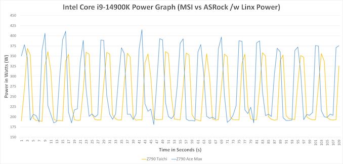
Pivoting to some real-world data highlighting these potential issues, when we reviewed the Intel Core i9-14900K, Intel's flagship Raptor Lake Refresh (RPL-R) processor, we tested with the default settings on both of our Z790 motherboards. From the above data, we can see the MSI MEG Z790 Ace Max was drawing up to 415 W when using Linx to place a very heavy workload on the chip. We also ran the same chip and workload on ASRock's Z790 Taichi Carrara to provide additional data points, where we found that it's power consumption maxed out at 375 W, around 10% lower than the MSI board.
In both cases, this is much higher than Intel's official PL2 limit for the Intel Core i9-14900K, which says that the chip should top out at 253 W for moderate periods of load. But, as we've seen time and time again, the official TDP ratings from Intel do not mean much to high-end motherboards, which almost universally default to higher settings. Motherboard vendors want to be competitive, and as such, higher default power settings allow vendors to claim that they deliver better performance than their rivals.
As further evidence of this, check out some of our recent motherboard reviews. I have assembled a small list of links to those reviews, where we've seen excessive CPU voltage or power consumption (or more often, both) when using the default settings on each motherboard, in each of the below reviews we see much higher power levels than Intel's official TDP values, which over the last several years we've come to expect. Still, some can be too high, especially with an already close-to-the-limit Core i9-14900K.
- ASRock Z790 Taichi Carrara Motherboard Review: ASRock Rocks With White Marble
- MSI MEG Z690 Unify (DDR5) Motherboard Review: The All-Black Option
- ASUS ROG Maximus XII Hero Wi-Fi Review: The Tale of Two Motherboards
We have been communicating with Intel for most of the day to get official answers to what's happening. We have, however received an official statement from Intel, which reads as follows:
The recently publicized communications between Intel and its motherboard partners regarding motherboard settings and Intel Core 13th & 14th Gen K-SKU processors is intended to provide guidance on Intel recommended default settings. We are continuing to investigate with our partners the recent user reports of instability in certain workloads on these processors.
This BIOS default settings guidance is meant to improve stability for currently installed processors while Intel continues investigating root cause, not ascribe blame to Intel's partners:
Intel Raptor Lake (13th)/Raptor Lake Refresh (14th) Gen K Series SKU Official Recommendations Parameter/Feature (In BIOS/Software Settings) Value/Setting Current Excursion Protection (CEP) Enable Enhanced Thermal Velocity Boost (eTVB) Enable Thermal Velocity Boost (TVB) Enable TVB Voltage Optimizations Enable ICCMAX Unlimited Bit Disable TjMAX Offset 0 C-states Enable ICCMAX Varies, Never >400A* ICCMAX_App Varies* Power Limits (PL's) Varies** Please see the 13th Generation Intel® Core™ and Intel® Core™ 14th Generation Processors datasheet for more information
Intel continues to work with its partners to develop appropriate mitigations going forward.
Intel's official statement to us, which is likely their standpoint for the general public, highlights a list of recommended BIOS and software settings, such as those found in Intel's Extreme Tuning Utility (XTU). There's no mention of specific motherboard vendors or models, but the above settings should alleviate crashing and instability issues by preventing motherboards from pushing CPUs too hard.
It remains to be seen just how motherboard vendors will opt to address the issue, as all of the motherboard vendors we contacted today didn't have anything official to say about the matter. With that said, however, a few motherboard vendors have recently released a wave of new BIOSes, adding a new profile called "Intel Baseline" or similar. In all cases, these new BIOSes seem to do exactly what it says on the label, configuring the system to run at Intel's actual, suggested stock settings, and thus ensuring the stability of system in exchange for reduced performance.
With that said, these new Intel baseline settings are still not being used as the default settings for high-end motherboards. So the out-of-the-box user experience is still for MCE and other features to be enabled, pushing these processors to their performance limit. Users who actually want baseline performance – and the guaranteed stability it comes with – will still need to go into the BIOS and explicitly select this profile.
Ultimately, given the spec-defying state of high-end motherboards over the last decade, this is a badly-needed improvement. But still, as Intel has yet to wrap up their root cause investigation and issue formal guidance to consumers, we're not quite to the end of this saga just yet. There are still some developments to come, as we expect to hear more in May.
The AlphaCool Core Ocean T38 360mm AIO CPU Cooler Review: Loud and Proud
Published: Apr 29nd 2024 9:30am on AnandTech
While the all-in-one CPU cooler industry is dominated, at least in mindshare, by flagship coolers from the industry’s biggest brands, the market segment overall has grown over the years to cover a much larger gamut of users. From flagship coolers to sub-$100 specials, effective AIO coolers have become available and affordable for most mid-range and higher builds. Thanks in part to some intensive competition in this space, we’ve seen several vendors bring down even 360mm coolers to the sub-$100 market in an effort to get in an edge over their competitors, and a sale in the process.
Looking at an opportunity to grow their own customer base, even the normally premium-focused AlphaCool has opted to get into this action with their Core Ocean lineup of coolers. And today, we're taking a closer look at the Core Ocean T38 360mm, AlphaCool's latest entry-level AIO cooler.
At a high level, the Core Ocean T38 has been designed to balance performance with manufacturing costs, allowing the company to put together an effective cooler that can still be priced low enough to reach budget-conscious consumers. Sticking with an aluminum radiator and keeping the frills such as RGB lighting to a minimum, the T38 is primarily aimed at system builders who require straightforward, effective cooling solutions – and without the complexity of AlphaCool's renowned open-loop custom liquid cooling kits. As we'll see, nothing comes for free, but AlphaCool has been able to put together a rather effective CPU cooler for $100 that's hard to ignore.
TSMC Jumps Into Silicon Photonics, Lays Out Roadmap For 12.8 Tbps COUPE On-Package Interconnect
Published: Apr 26nd 2024 4:00am on AnandTech
Optical connectivity – and especially silicon photonics – is expected to become a crucial technology to enable connectivity for next-generation datacenters, particularly those designed HPC applications. With ever-increasing bandwidth requirements needed to keep up with (and keep scaling out) system performance, copper signaling alone won't be enough to keep up. To that end, several companies are developing silicon photonics solutions, including fab providers like TSMC, who this week outlined its 3D Optical Engine roadmap as part of its 2024 North American Technology Symposium, laying out its plan to bring up to 12.8 Tbps optical connectivity to TSMC-fabbed processors.
TSMC's Compact Universal Photonic Engine (COUPE) stacks an electronics integrated circuit on photonic integrated circuit (EIC-on-PIC) using the company's SoIC-X packaging technology. The foundry says that usage of its SoIC-X enables the lowest impedance at the die-to-die interface and therefore the highest energy efficiency. The EIC itself is produced at a 65nm-class process technology.
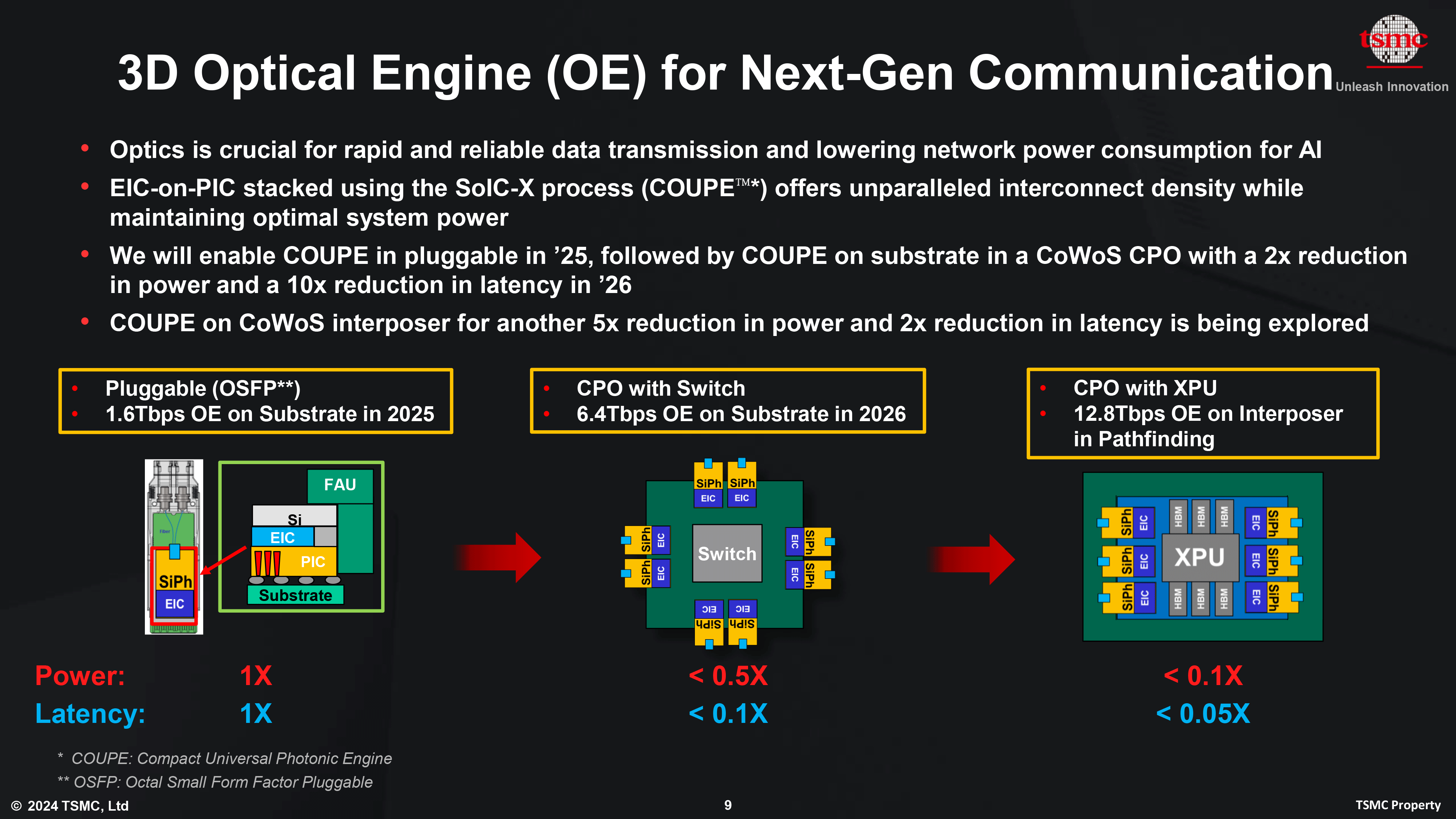
TSMC's 1st Generation 3D Optical Engine (or COUPE) will be integrated into an OSFP pluggable device running at 1.6 Tbps. That's a transfer rate well ahead of current copper Ethernet standards – which top out at 800 Gbps – underscoring the immediate bandwidth advantage of optical interconnects for heavily-networked compute clusters, never mind the expected power savings.
Looking further ahead, the 2nd Generation of COUPE is designed to integrate into CoWoS packaging as co-packaged optics with a switch, allowing optical interconnections to be brought to the motherboard level. This version COUPE will support data transfer rates of up to 6.40 Tbps with reduced latency compared to the first version.
TSMC's third iteration of COUPE – COUPE running on a CoWoS interposer – is projected to improve on things one step further, increasing transfer rates to 12.8 Tbps while bringing optical connectivity even closer to the processor itself. At present, COUPE-on-CoWoS is in the pathfinding stage of development and TSMC does not have a target date set.
Ultimately, unlike many of its industry peers, TSMC has not participated in the silicon photonics market up until now, leaving this to players like GlobalFoundries. But with its 3D Optical Engine Strategy, the company will enter this important market as it looks to make up for lost time.
Related Reading- TSMC's 1.6nm Technology Announced for Late 2026: A16 with "Super Power Rail" Backside Power
- TSMC 2nm Update: N2 In 2025, N2P Loses Backside Power, and NanoFlex Brings Optimal Cells
- TSMC Preps Cheaper 4nm N4C Process For 2025, Aiming For 8.5% Cost Reduction
- TSMC's System-on-Wafer Platform Goes 3D: CoW-SoW Stacks Up the Chips
TSMC Preps Cheaper 4nm N4C Process For 2025, Aiming For 8.5% Cost Reduction
Published: Apr 25nd 2024 10:00am on AnandTech
While the bulk of attention on TSMC is aimed at its leading-edge nodes, such as N3E and N2, loads of chips will continue to be made using more mature and proven process technologies for years to come. Which is why TSMC has continued to refine its existing nodes, including its current-generation 5nm-class offerings. To that end, at its North American Technology Symposium 2024, the company introduced a new, optimized 5nm-class node: N4C.
TSMC's N4C process belongs to the company's 5nm-class family of fab nodes and is a superset of N4P, the most advanced technology in that family. In a bid to further bring down 5nm manufacturing costs, for TSMC is implementing several changes for N4C, including rearchitecting their standard cell and SRAM cell, changing some design rules, and reducing the number of masking layers. As a result of these improvements, the company expects N4C to achieve both smaller die sizes as well as a reduction in production complexity, which in turn will bring die costs down by up to 8.5%. Furthermore, with the same wafer-level defect density rate as N4P, N4C stands to offer even higher functional yields thanks to its die area reduction.
"So, we are not done with our 5nm and 4nm [technologies]," said Kevin Zhang, Vice President of Business Development at TSMC. "From N5 to N4, we have achieved 4% density improvement optical shrink, and we continue to enhance the transistor performance. Now we bring in N4C to our 4 nm technology portfolio. N4C allows our customers to reduce their costs by remove some of the masks and to also improve on the original IP design like a standard cell and SRAM to further reduce the overall product level cost of ownership."
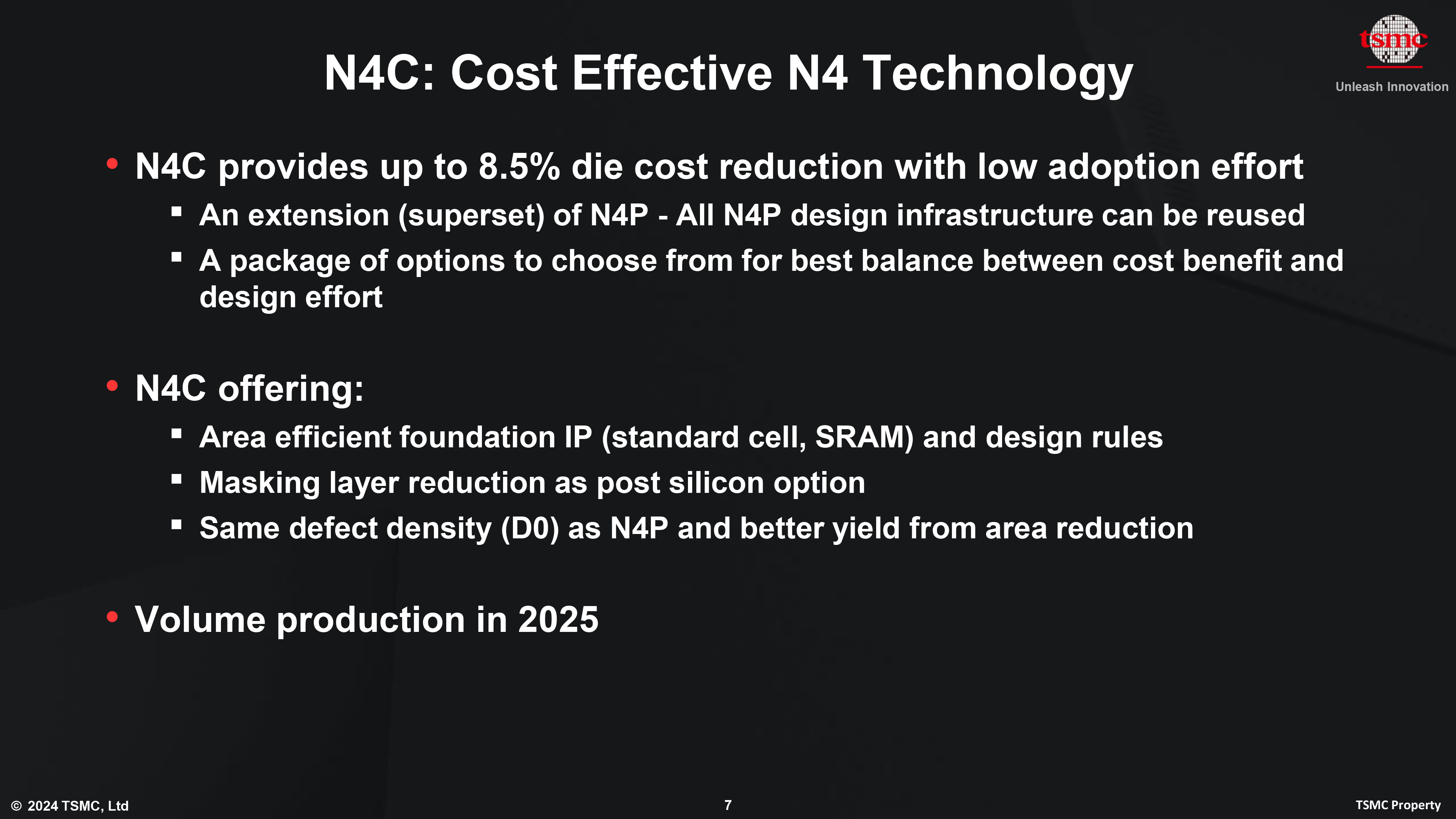
TSMC says that N4C can use the same design infrastructure as N4P, though it is unclear whether N5 and N4P IP can be re-used for N4C-based chips. Meanwhile, TSMC indicates that it offers various options for chipmakers to find the right balance between cost benefits and design effort, so companies interested in adopting a 4nm-class process technologies could well adopt N4C.
The development of N4C comes as many of TSMC's chip design customers are preparing to launch chips based on the company's final generation of FinFET process technology, the 3nm N3 series. While N3 is expected to be a successful family, the high costs of N3B have been an issue, and the generation is marked by diminishing performance and transistor density returns altogether. Consequently, N4C could well become a major, long-lived node at TSMC, serving as a good fit for customers who want to stick to a more cost-effective FinFET node.
"This is a very significant enhancement, we are working with our customer, basically to extract more value from their 4 nm investment," Zhang said.
TSMC expects to start volume production of N4C chips some time next year. And with TSMC having produced 5nm-class for nearly half a decade at that point, N4C should be able to hit the ground running in terms of volume and yields.
Related Reading