Lenovo Unveils Yoga Slim 7x 14 Gen 14 and ThinkPad T14 Gen 6 Notebooks Powered By Qualcomm Snapdragon X Elite
Published: May 20nd 2024 2:00am on AnandTech
While we've been expecting the availability of the Qualcomm Snapdragon X Elite processor to be around the middle of this year, Lenovo has announced two new 'AI-powered' notebooks for the Windows on Arm platform. Announced is the Lenovo Yoga Slim 7x Gen 14 and the Lenovo ThinkPad T14s Gen 6 both feature Qualcomm's latest 12-core Snapdragon X Elite processor, ushering in a new era for Microsoft's Windows on Arm platform. Lenovo aims to target content creators and business professionals with these new models.
Qualcomm's new Snapdragon X Elite processor looks set to try to change the adoption of the Windows-on-Arm devices, with a critical focus on providing AI capability on device, which promises up to 45 TOPs of performance solely from the Hexagon NPU. Powered by the Oryon CPU cores, the Snapdragon X Elite is designed to deliver exceptional performance and efficiency, achieving up to 3.8GHz in all-core turbo in intensive workloads. The processor also includes the latest Hexagon NPU, offering 45 TOPS of performance for INT8 tasks, making it well-suited for handling complex AI tasks on devices such as Generative AI.
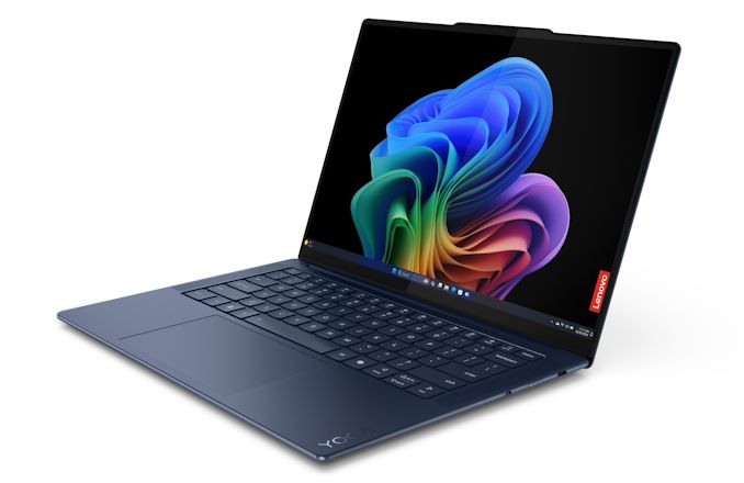 Lenovo Yoga Slim 7x Gen 14 Notebook for Windows on Arm
Starting with the slimmer of the two models, the Lenovo Yoga Slim 7x is primarily tailored for creators. It is designed to be thin, lightweight, and portable and has a 70 Wh battery, making it ideal for creators on the go. The device is powered by the latest Snapdragon X Elite processor, featuring Qualcomm's integrated Hegaxon NPU designed to power GenAI-based text-to-image capabilities, sophisticated photo and video editing tools, and intelligent text creation and editing feedback.
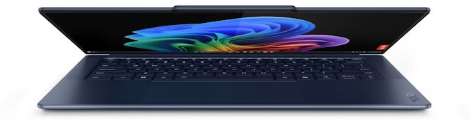 The Lenovo Yoga Slim 7x Gen 14 is just 12.9 mm thick.
For connectivity, it only uses Type-C, with three USB 4 Type-C ports for the fastest 40 Gbps-capable devices. It also has a single audio jack with an HDMI 2.1 video output. Built into the top bezel is a 1080 webcam with four microphones, and it also supports IP MIPI with an integrated privacy shutter. Additional features include Dolby Atmos audio, while it also comes with Wi-Fi 7 and Bluetooth 5.3 connectivity incorporated within the Qualcomm Snapdragon X Elite processor. It weighs just 1.28 kg, with a slim 12.9 mm profile, making the Lenovo Yoga Slim 7x perfectly light for users on the go.
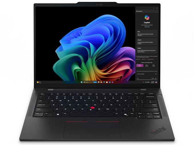
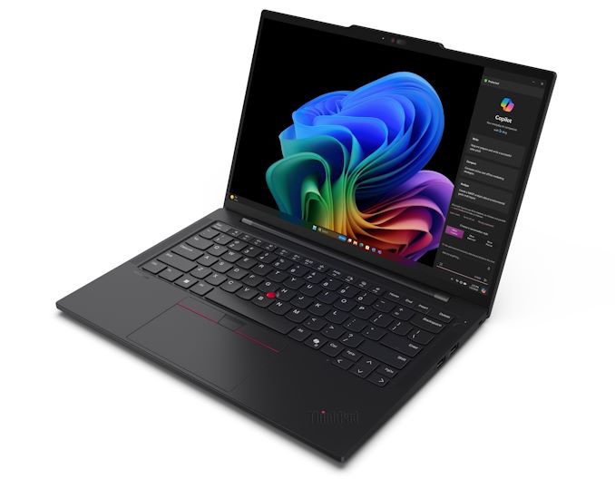 The Lenovo ThinkPad T14s Gen 6 notebook
On the other hand, the Lenovo ThinkPad T14s is optimized primarily for business users. It is designed to deliver optimal performance and efficiency with the Qualcomm Snapdragon X Elite 12-core processor. As with the Yoga Slim 7x, the ThinkPad T14s uses the integrated Qualcomm Adreno GPU for graphics capabilities, and it powers the 14" display, which can come in 1920 x 1200 IPS or 2.8K with an OLED panel. The on-device Hexagon NPU primarily handles AI inferencing tasks on chips and ensures seamless integration with Microsoft 365 applications. This model is designed to provide robust device management, enhanced collaborations on the go, and integrated chip-to-cloud security for professional environments.
Lenovo ThinkPad T14s Gen 6 & Yoga Slim 7x 14 Gen 9 Specifications (Qualcomm Snapdragon X Elite Models) AnandTech ThinkPad T14s Gen 6 Yoga Slim 7x 14 Gen 9 Processor Qualcomm Snapdragon X Elite Windows on Arm 12C / 12 T Up to 3.8 GHz All-Core 4.2 GHz 2T Boost Dynamic undisclosed TDP Qualcomm Snapdragon X Elite Windows on Arm 12C / 12 T Up to 3.4 GHz All-Core 4.0 GHz 2T Boost Dynamic undisclosed TDP Memory Up to 64 GB LPRRD5X-8533 2 x 32 GB Up to 32 GB LPRRD5X-8448 2 x 16 GB GPU Qualcomm Snapdragon X Elite Adreno Graphics NPU Qualcomm Hexagon NPU (45 TOPS) Display 14" IPS, 1920 x 1200, sRGB, 400 nits 14" IPS, 1920 x 1200, NTSC, 400 nits 14" OLED, 2.8k, HDR5x, 400 nits 14.5" OLED, 2944 x 1840, 90Hz, Touch Storage Up to 1 TB PCIe 4.0 x4 Up to 1 TB PCIe 4.0 x4 Networking Wi-Fi 7 Bluetooth 5.3 Wi-Fi 7 Bluetooth 5.3 Audio Dual Speakers, Dolby Audio Dolby Atmos Battery 58 Wh (No battery runtime claimed) 70 Wh (No battery runtime claimed) Connectivity 2 x USB 3.2 G2 Type-A 2 x USB 4 Type-C Audio Jack HDMI 2.1 Output 3 x USB 4 Type-C, PD 3.1, DP 1.4 Dimensions 313.6 x 219.4 x 16.9 mm (12.34 x 8.64 x 0.67 inches) 325 x 225.15 x 12.9 mm (12.8 x 8.86 x 0.51 inches) Weight 1.24 kg / 2.72 lb 1.28 kg / 2.82 lb Camera 1080p, IR MIPI /w Privacy Shutter 1080p, IR MIPI /w Privacy Shutter Color Eclipse Black Cosmic Blue Pricing Starting From $1699 Starting From $1199On the connectivity front, it has dual USB 3.2 G2 Type-A ports and two USB 4 Type-C ports for the fastest 40 Gbps-capable devices. It also has a single audio jack with an HDMI 2.1 video output. Built into the top bezel is a 1080 webcam with dual microphones, and it also supports IP MIPI with an integrated privacy shutter. Additional features include a fingerprint reader within the power button and dTPM. Lenovo uses the integrated Wi-Fi 7 within the Snapdragon X Elite for wireless connectivity, providing Bluetooth 5.3 support.
The Lenovo Yoga Slim 7x 14 Gen 9 and ThinkPad T14s Gen 6 can support up to 1TB of PCIe 4.0 x4 storage, while memory capability depends on the model. The Yoga 7x 14 Gen 9, a slimmer model, is limited to 32 GB of LPDDR5X-8448 memory in a dual-channel configuration. At the same time, the ThinkPad T14s Gen 6 can accommodate up to 64 GB of slightly faster LPDDR5X-8533 memory.
Additionally, Lenovo offers deployment services through its Lenovo TruScale platform to support the efficient management of next-generation AI PC devices such as these models. These services include customizable security features, tailored deployment processes, enhanced control over the deployment process, and services designed to align with specific business objectives.
Both the Lenovo Yoga Slim 7x and the Lenovo ThinkPad T14s Gen 6 will be available starting June 2024, with the Yoga Slim 7x starting at $1,199 and the ThinkPad T14s Gen 6 priced starting at $1,699.
Gallery: Lenovo Unveils Yoga Slim 7x and ThinkPad T14 Gen 6 Powered By Qualcomm Snapdragon X Elite


Intel Teases Lunar Lake CPU Ahead of Computex: Most Power Efficient x86 Chip Yet
Published: May 20nd 2024 2:00am on AnandTech
The next few weeks in the PC industry are going to come fast and furious. Between today and mid-June are multiple conferences and trade-shows, including Microsoft Build and the king of PC trade shows: Computex Taiwan. With all three PC CPU vendors set to present, there’s a lot going on, and a lot of product announcements to be had. But even before those trade shows start, Intel is looking to make the first move this afternoon with an early preview on its next-gen mobile processor, Lunar Lake.
While Intel hasn’t said too much about what to expect from their Computex 2024 keynote thus far, it’s clear that Intel’s next-gen CPUs – Lunar Lake for mobile, and Arrow Lake for Mobile/Desktop – are going to be two of the major stars of the show. At this point Intel has previously teased and/or demoed both chips (Lunar more so than Arrow), and this afternoon the company is releasing a bit more information on Lunar Lake even before Computex kicks off.
Officially, today’s reveal is a preview of Intel’s next Tech Tour event, which is taking place at the end of May. Unofficially, this is the exact same date and time as the embargo on Qualcomm Snapdragon X laptop announcements, which are slated to hit retail shelves next month. Lunar Lake laptops, by contrast, will not hit retail shelves until Q4 of this year. So although the additional technical details from today’s disclosure are great to have, looking at the bigger picture it’s difficult to interpret this reveal as anything less than a bald-faced effort to interdict the Snapdragon X launch (not that Qualcomm hasn’t also been crowing about SDX for the last 7 months). Which, if nothing else, goes to show the current tumultuous state of the laptop CPU market, and that Intel isn’t nearly as secure in their position as they have traditionally been.
TSMC Outlines Path to EUV Success: More Tools, More Wafers, & Best Pellicles In Industry
Published: May 17nd 2024 2:00am on AnandTech
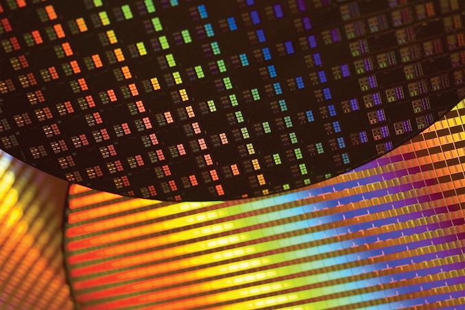
Although TSMC can't claim to be the first fab to use extreme UV (EUV) lithography – that title goes to Samsung – they do get to claim to be the largest. As a result, the company has developed significant experience with EUV over the years, allowing TSMC to refine how they use EUV tooling to both improve productivity/uptime, and to cut down on the costs of using the ultra-fine tools. As part of the company's European Technology Symposium this week, they went into a bit more detail on their EUV usage history, and their progress on further integrating EUV into future process nodes.
When TSMC started making chips using EUV lithography in 2019 on its N7+ process (for Huawei's HiSilicon), it held 42% of the world's installed base of EUV tools, and even as ASML ramped up shipments of EUV scanners in 2020, TSMC's share of EUV installations actually increased to 50%. And jumping ahead to 2024, where the number of EUV litho systems at TSMC has increased by 10-fold from 2019, TSMC is now 56% of the global EUV installed base, despite Samsung and Intel ramping up their own EUV production. Suffice it to say, TSMC made a decision to go in hard on EUV early on, and as a result they still have the lion's share of EUV scanners today.
Notably, TSMC's EUV wafer production has increased by an even larger factor; TSMC now pumps out 30 times as many EUV wafers as they did in 2019. Compared to the mere 10x increase in tools, TSMC's 30x jump in production underscores how TSMC has been able to increase their EUV productivity, reduce service times, and fewer tool downtimes overall. Apparently, this has all been accomplished using the company's in-house developed innovations.
TSMC's Leadership in EUV High Volume Manufacturing Data by TSMC (Compiled by AnandTech) 2019 2023 Cumulative Tools 1X 10X Share of Global EUV Installed Base 42% 56% EUV Wafer Output 1X 30X Wafer per Day per EUV Tool 1X 2X Reticle Particle Contamination 1X 0.1XTSMC says that it has managed to increase wafer-per-day-per-tool productivity of its EUV systems by two times since 2019. To do so, the company optimized the EUV exposure dose and the photoresist it uses. In addition, TSMC greatly refined its pellicles for EUV reticles, which increased their lifespan by four times (i.e., increases uptime), increased output per pellicle by 4.5 times, and lowered defectivity by massive 80 times (i.e., improves productivity and increases uptime). For obvious reasons, TSMC does not disclose how it managed to improve its pellicle technology so significantly, but perhaps over time the company's engineers are going to share this with academia.
TSMC's EUV Pellicle Technology vs. Commercial Data by TSMC (Compiled by AnandTech) Commercial TSMC (Claimed) Output 1X 4.5X Defectivity 1X 0.0125X Lifespan 1X 4XEUV lithography systems are also notorious for their power consumption. So, in addition to improving productivity of EUV tools, the company also managed to reduce the power consumption of its EUV scanners by 24% through undisclosed 'innovative energy saving techniques.' And the company isn't done there: they are planning to improve energy efficiency per wafer per EUV tool by 1.5 times by 2030.
Considering all the refinements that TSMC has managed to achieve with Low-NA EUV lithography by now, it is not terribly surprising that the company is quite confident that it can continue to produce cutting-edge chips in the future. Whereas rival Intel has gone all-in on High-NA EUV for their future, sub-18A nodes, TSMC is looking to leverage their highly-optimized and time-tested Low-NA EUV tooling instead, avoiding the potential pitfalls of a major technology transition so soon while also reaping the cost benefits of using the well-established tooling.
Capsule Review: Sunon Maglev 120mm Fan
Published: May 17nd 2024 1:00am on AnandTech
Founded in 1980 and headquartered in Taiwan, Sunon (aka Sunonwealth Electric Machine Industry Co., Ltd.), stands out as a prominent global producer of fans, blowers, and thermal management systems. The company has made a name for itself in the fan industry with a comprehensive product line that includes DC brushless fans, micro blowers, CPU coolers, and various other cooling technologies. They are one of the oldest and most renowned fan manufacturers on the world – and not just for PC applications, but for just about anything in need of something smaller than a ceiling fan, spanning from IT to automotive and industrial sectors.
Within the PC space, the company is best known for its proprietary MagLev (Magnetic Levitation) technology, which uses magnetic forces to levitate the rotor shaft, drastically reducing friction and wear. This innovative design improves the durability and performance of their fans, particularly in reducing operational noise and improving high-temperature performance. Sunon introduced the patent and their first MagLev products all the way back in 90s.
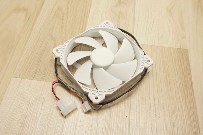
The 120mm Sunon MagLev fan (MFC0251V2-1Q02U-S99) that we are reviewing today is a new, high-performance fan engineered primarily for PC applications, with an emphasis on longevity and functionality. It features Sunon's advanced Vapo-Bearing MagLev Engine, which allegedly ensures a quieter operation and longer lifespan by minimizing friction. This particular fan has a maximum speed of 1900 RPM and all of the bells and whistles of advanced cooling fans, including a wide range PWM speed control (10-100%).
Distinguished by its crisp white color and unique frame design, this fan is aimed PC builders going for a clean and modern aesthetic. The "gaming" designation by the manufacturer clearly divulges their intentions regarding their targeted audience. By default, these fans have both a 4-pin connector and also a Molex connector for their direct connection to the PSU.
Fan Testing Methodology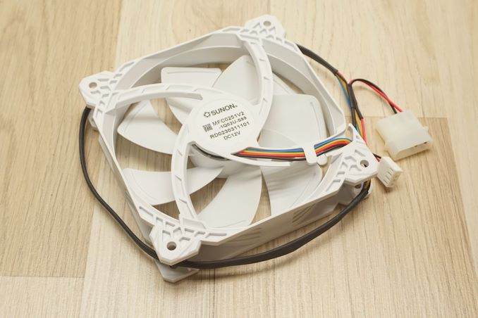

We are testing fans using an Extech HD350 differential manometer, an Extech AN200 velocity meter, and a custom 3D printed apparatus designed for this specific purpose. The apparatus features a simple but effective shutters mechanism that allows us to test the unobstructed (maximum) volume flow of a fan, the fully obstructed (maximum static) pressure of the fan, and multiple points in between, allowing us to compose the actual P-Q performance chart of any fan. The RPM reading is taken with the fan unobstructed (maximum flow), as the fan speed varies depending on the airflow impedance in conjunction with the design of the fan’s blades.
For noise measurements, we are using an Extech HD600 high sensitivity SPL meter. The noise of the fan is measured from 15 centimeters away, not one meter as IEC certifications require, as that would be far too great a distance to measure differences between nearly silent products. Note however that we are measuring the noise level of a fan with its flow unobstructed and the fan, to the best possible degree, uncoupled from the environment. The addition of fan grills, the installation on a cooler, and any other form of obstruction will increase the generated noise, as both aerodynamic and vibration noise will be added into the environment.
Test Results & Conclusion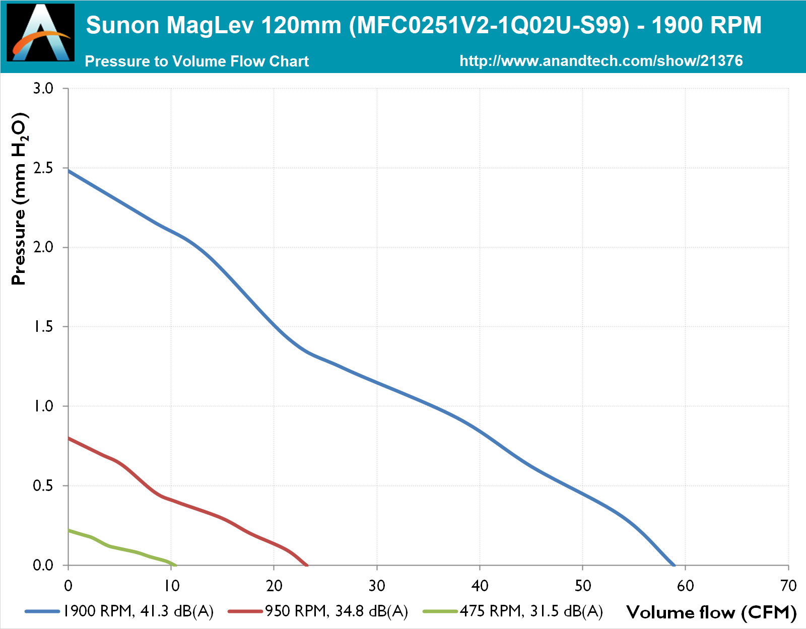
The Sunon MFC0251V2-1Q02U-S99 is a robust performer across the entirety of the performance chart. At its maximum speed of 1900 RPM, it offers an airflow of 58.9 CFM and a static pressure of 2.48 mmH2O. However, that performance comes with a noise output of 41.3 dB(A), which is quite noticeable and, in most cases, not really ahead of its competition. When compared to the Corsair ML120, another fan with a magnetic levitation engine, the Sunon model tends to offer significantly better performance by running about 300 RPM faster while generating about the same level of noise.
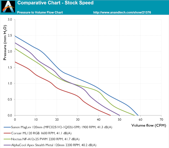
Overall, Sunon's 120mm MagLev fan stands out as a high-quality part, and better still it's priced competitively at around $11, offering substantial value for those looking for robust cooling solutions within budget constraints. When it's used correctly, the fan easily competes with, and generally outperforms, the best 120 mm products currently available – albeit not immensely so.
However "used correctly" is the operative term, as the MagLev engine makes the fan particular about its orientation. In short, these fans are not meant to be installed with the engine facing upwards, as this can jeopardize the integrity of the Vapo mechanism. As a result, Sunon's MagLev fan is really only good for horizontal uses – front and back air intake/exhaust – and shouldn't be used for vertical configurations at the top and bottom of computer cases.
Despite that, the 120mm MagLev fan does excel when it's in its niche, especially at its price. The biggest hurdle, in that case, is just acquiring a fan, as Sunon is primarily geared up to target the bulk OEM market and doesn't sell their fans in individual retail units. So prospective buyers will need to skip the Neweggs and Amazons of the world, and look instead at electronic and industrial suppliers like Digikey and Mouser.
Not Dead Yet: WD Releases New 6TB 2.5-Inch External Hard Drives - First Upgrade in Seven Years
Published: May 16nd 2024 7:00am on AnandTech
The vast majority of laptops nowadays use solid-state drives, which is why the development of new, higher-capacity 2.5-inch hard drives has all but come to a halt. Or rather, it almost has. It seems that the 2.5-inch form factor has a bit more life left in it after all, as today Western Digital has released a slate of new external storage products based on a new, high-capacity 6 TB 2.5-inch hard drive.
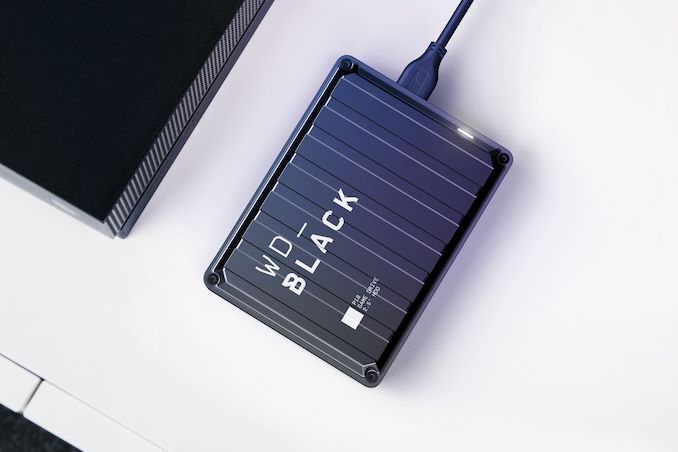
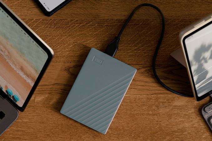
WD's new 6 TB spinner is being used to offer upgraded versions of the company's My Passport, Black P10, and and G-DRIVE ArmorATD portable storage products. Notably, however, WD isn't selling the bare 2.5-inch drive on a standalone basis – at least not yet – so for the time being it's entirely reserved for use in external storage.
Consequently, WD isn't publishing much about the 6 TB hard drive itself. The maximum read speed for these products is listed at 130 MB/sec – the same as WD's existing externals – and write performance goes unmentioned.
Notably, all of these 6 TB devices are thicker than their existing 5 TB counterparts, which strongly suggests that WD has increased their storage capacity not by improving their areal density, but by adding another platter to their existing drive platform. This, in turn, would help to explain why these new drives are being used in external storage products, as WD's 5 TB 2.5-inch drives are already 15mm thick, which is the highest standard thickness for a 2.5-inch form-factor, and already incompatible with a decent number of portable devices. External drives, in turn, are the only place these even thicker 2.5-inch drives would fit.
WD's specifications also gloss over whether these drives are based on shingled magnetic recording (SMR) technology. The company was already using SMR for their 5 TB drives in order to hit the necessary storage density there, so it seems very likely that they're continuing to use SMR for their 6 TB drives. Which is likely why the company isn't publishing write performance specifications for the drives, as we've seen SMR drives bottom out as low as 10 MB/second in our testing when the drive needs to rewrite data.
Depending on the specific drive model, all of the external storage drives use either a USB-C connector, or the very quaint USB Micro-B 3.0 connector. Though regardless of the physical connector used, all of the drives feature a USB 3.2 Gen 1 (5Gbps) interface, which is more than ample given the drives' physically-limited transfer speeds.
Wrapping things up, according to WD the new drives are available at retail immediately. The WD My Passport Ultra and WD My Passport Ultra for Mac with USB-C both retail for $199.99; the WD My Passport and WD My Passport for Mac are $179.99; the WD My Passport Works With USB-C is $184.99; the gaming-focused WD_Black P10 Game Drive sells for $184.99, and the SanDisk Professional G-Drive ArmorATD is $229.99. All of Western Digital's external storage drives are backed with a three-year limited warranty.
TSMC to Expand Specialty Capacity by 50%, Introduce 4nm N4e Low-Power Node
Published: May 16nd 2024 5:00am on AnandTech

With all the new fabs being built in Germany and Japan, as well as the expansion of production capacity in China, TSMC is planning to extend its production capacity for specialty technologies by 50% by 2027. As disclosed by the company during its European Technology Symposium this week, TSMC expects to need to not only convert existing capacity to meet demands for specialty processes, but even build new (greenfield) fab space just for this purpose. One of the big drivers for this demand, in turn, will be TSMC's next specialty node: N4e, a 4nm-class ultra-low-power production node.
"In the past, we always did the review phase [for upcoming fabs], but for the first time in a long time at TSMC, we started building greenfield fab that will address the future specialty technology requirements," said Dr. Kevin Zhang, Senior Vice President, Business Development and Overseas Operations Office, at the event. "In the next four to five years, we actually going to grow our specialty capacity by up to 1.5x. In doing so we actually expanding the footprint of our manufacturing network to improve the resiliency of the overall fab supply chain."
On top of its well-known major logic nodes like N5 and N3E, TSMC also offers a suite of specialty nodes for applications such as power semiconductors, mixed analog I/O, and ultra-low-power applications (e.g. IoT). These are typically based on the company's trailing manufacturing processes, but regardless of the underlying technology, the capacity demand for these nodes is growing right alongside the demand for TSMC's major logic nodes. All of which has required TSMC to reevaluate how they go about planning for capacity on their specialty nodes.
TSMC's expansion strategy in the recent years has pursued several goals. One of them has been to build new fabs outside of Taiwan; another has been to generally expand production capacity to meet future demand for all types of process technologies – which is why the company is building up capacity for specialty nodes.
At present, TSMC's most advanced specialty node is N6e, an N7/N6 variant that supports operating voltages between 0.4V and 0.9V. With N4e, TSMC is looking at voltages below 0.4V. Though for now, TSMC is not disclosing much in the way of technical details for the planned node; given the company's history here, we expect they'll have more to talk about next year once the new process is ready.
The Arctic Cooling Freezer 36 ARGB CPU Cooler Review: Budget Cooling Done Well
Published: May 16nd 2024 9:00am on AnandTech
As modern high-performance CPUs generate more heat, there's been a noticeable increase in the demand for powerful air coolers capable of managing these thermal challenges. Traditional stock air coolers, while sufficient for regular use, are typically designed to be cheap and relatively compact, leaving further improvements to noise control and peak cooling efficiency on the table. This gap has long prompted advanced users and system builders to opt for high-quality aftermarket coolers that designed to better handle the heat output from top-tier processors.
Known for their innovative approach to PC hardware, Arctic Cooling has stepped into this competitive market with a product aimed at delivering effective cooling at a very low retail price. The Freezer 36 A-RGB, a dual fan tower cooler, is designed to support the cooling demands of the latest CPUs while also offering customizable RGB lighting for visual flair. This review will explore the features, performance, and value of the Arctic Cooling Freezer 36 A-RGB, comparing it with other leading products in the market to see how it stacks up in providing efficient and effective cooling for modern CPUs.
TSMC Readies Next-Gen HBM4 Base Dies, Built on 12nm and 5nm Nodes
Published: May 16nd 2024 8:00am on AnandTech

Of the several major changes coming with HBM4 memory, one of the most immediate is the sheer width of the memory interface. With the fourth-generation memory standard moving from an already wide 1024-bit interface to a ultra-wide 2048-bit interface, HBM4 memory stacks won't be business as usual; chip manufacturers are going to need to adopt more advanced packaging methods than are used today to accommodate the wider memory.
As part of its European Technology Symposium 2024 presentation, TSMC offered some fresh details into the base dies it will be manufacturing for HBM4, which will be built using logic processes. With TSMC planning to employ variations of their N12 and N5 processes for this task, the company is expecting to occupy a favorable place in the HBM4 manufacturing process, as memory fabs are not currently equipped to economically produce such advanced logic dies – if they can produce them at all.
For the first wave of HBM4, TSMC is preparing to use two fabrication processes: N12FFC+ and N5. While they serve the same purpose — integrating HBM4E memory with next-generation AI and HPC processors — they are going to be used in two different ways to connect memory for high-performance processors for AI and HPC applications.
"We are working with key HBM memory partners (Micron, Samsung, SK Hynix) over advanced nodes for HBM4 full stack integration," said Senior Director of Design and Technology Platform at TSMC. "N12FFC+ cost effective base die can reach HBM for performance and N5 base die can provide even more logic with much lower power at HBM4 speeds."
TSMC Logic for HBM4 Base Die N12FFC+ N5 Area 1X 0.39X Logic GHz @ power 1X 1.55X Power @ GHz 1X 0.35XTSMC's base die made on N12FFC+ fabrication process (12nm FinFet Compact Plus, which formally belongs to a 12nm-class technology, but it lays its roots from TSMC's well-proven 16nm FinFET production node) will be used to install HBM4 memory stacks on a silicon interposer next to system-on-chips (SoCs). TSMC believes that their 12FFC+ process is well-suited to achieve HBM4 performance, enabling memory vendors to build 12-Hi(48 GB) and 16-Hi stacks (64 GB), with per-stack bandwidth well as over 2 TB/second.
"We are also optimizing CoWoS-L and CoWoS-R for HBM4," the Senior Director said. "Both CoWoS-L and CoWoS-R [use] over eight layers to enable HBM4's routing of over 2,000 interconnects with [proper] signal integrity."
HBM4 base dies on N12FFC+ will be instrumental in building system-in-packages (SiPs) using TSMC's CoWoS-L or CoWoS-R advanced packaging technology, which offer interposers up to 8x reticle size – enough space for up to 12 HBM4 memory stacks. At present, HBM4 can achieve data transfer rates of 6 GT/s at currents of 14mA, according to TSMC figures.
"We collaborate with EDA partners like Cadence, Synopsys, and Ansys to certify HBM4 channel signal integrity, IR/EM, and thermal accuracy," the TSMC representative explained.
Meanwhile, as an even more advanced alternative, memory manufacturers will also have the option of tapping TSMC's N5 process for their HBM4 base dies. N5-built base dies will pack even more logic, consume less power, and will offer even higher performance. But arguably the most important benefit is that such an advanced process technology will enable are very small interconnect pitches, on the order of 6 to 9 microns. This will allow N5 base dies to be used in conjunction with direct bonding, enabling HBM4 to be 3D stacked right on top of logic chips. Direct bonding stands to allow for even greater memory performance, which is expected to be a big boost for AI and HPC chips that are always scrounging for more memory bandwidth.
We already know that TSMC and SK Hynix collaborate on HBM4 base dies. It is likely that TSMC will also produce HBM4 base dies for Micron. Otherwise, we'd be more surprised to see TSMC working with Samsung, as that conglomerate already has its own advanced logic fabs via its Samsung Foundry unit.
TSMC: Performance-Optimized 3nm N3P Process on Track for Mass Production This Year
Published: May 15nd 2024 6:00am on AnandTech
As part of the second leg of TSMC's spring technology symposium series, the company offered an update on the state of its 3nm-class processes, both current and future. Building on the back of their current-generation N3E process, the optical shrink of this process technology, N3P, is now on track to enter mass production in the second half of 2024. Thanks to that shrink, N3P is expected to offer both increased performance efficiency as well as increased transistor density over N3E.
N3E in Production, Yielding WellWith N3E already in volume production, TSMC is reporting that they're seeing "great" yields on the second-generation 3nm-class process note. According to the company, the D0 defect density of N3E is at relative parity with N5, matching the defect rate of the older node for the same point in its respective lifecycle. This is no small feat, given the additional complexities that come with developing one last, ever-finer generation of FinFET technology. So for TSMC's bleeding-edge customers such as Apple, who just launched their M4 SoC, this is allowing them to reap the benefits of the improved process node relatively quickly.
"N3E started volume production in the fourth quarter of last year, as planned," a TSMC executive said at the event. "We have seen great yield performance on customers' products, so they did go to market as planned."
TSMC's N3E node is a relaxed version of N3B, eliminating some EUV layers and completely avoiding the usage of EUV double patterning. This makes it a bit cheaper to produce, and in some cases it widens the process window and yields, though it comes at the cost of some transistor density.
N3P on Track For Second-Half 2024Meanwhile, looking towards the immediate future at TSMC, N3P has finished qualification and its yield performance is close to N3E, according to the company. Being an optical shrink, the N3P node is set to enable processor developers to either increase performance by 4% at the same leakage or reduce power consumption by 9% at the same clocks (previously the range was between 4% ~ 10% depending on design). The new node is also set to boost transistor density by 4% for a 'mixed' chip design, which TSMC defines as a processor consisting of 50% logic, 30% SRAM, and 20% analog circuits.
Advertised PPA Improvements of New Process Technologies Data announced during conference calls, events, press briefings and press releases TSMC N3 vs N5 N3E vs N5 N3P vs N3E N3X vs N3P Power -25-30% -32% -5% ~ 10% higher Performance +10-15% +18% +5% +5% Fmax @ 1.2V Chip Density ? ? 1.04x same SRAM Cell Size 0.0199µm² (-5% vs N5) 0.021µm² (same as N5) ? ? Volume Manufacturing Late 2022 H2 2023 H2 2024 2025While it looks like the original N3 (aka N3B) will have a relatively muted lifecycle since Apple has been its only major customer, N3E will be adopted by a wide range of TSMC's customers, which includes many of the industry's biggest chip designers.
Since N3P is an optical shrink of N3E, it is compatible with its predecessor in terms of IP blocks, process rules, electronic design automation (EDA) tools, and design methodology. As a result, TSMC expects the majority of new tape outs to use N3P, not N3E or N3. This is logical as N3P provides higher performance efficiency than N3E at a lower cost than N3.
The most important aspect of N3P is that it is on track to be production ready in the second half of this year, so expect chip designers to adopt it straight away.
"We have also successfully delivered N3P technology," the TSMC executive said. "It has passed qualification and yield performance is close to N3E. [The process technology] has also received product customer tape outs and will start on production in the second half of this year. Because of [PPA advantages] of N3P, we expect the majority of tape outs on N3 to go to N3P."
Supermicro E102-13R-H Review: A Raptor Lake-P 3.5" SBC System for Embedded Applications
Published: May 14nd 2024 8:00am on AnandTech
Single-board computers in the 3.5" form-factor have become extremely popular for embedded applications involving a mix of high performance requirements as well as extended peripherals support. Typical use-case scenarios include digital signage, edge inferencing solutions, retail applications, and IoT gateways. The requirements in these segments call for processors and components that can operate in a wide temperature range. The chassis and cooling solution handle other duties such as ruggedness and avoidance of moving parts. The Supermicro X13SRN-H-WOHS is a 3.5" SBC with a soldered-down Intel Core i7-1370PE - a Raptor Lake-P embedded processor with vPro support. It has plenty of I/O support, including a SlimSAS PCIe expansion slot. Supermicro also offers a ready-to-deploy solution using the SBC in the actively-cooled SYS-E102-13R-H box PC. This review takes a detailed look at the features and performance profile of the SYS-E102-13R-H, along with an evaluation of the thermal solution.