TSMC: Performance and Yields of 2nm on Track, Mass Production To Start In 2025
Published: May 30nd 2024 3:00am on AnandTech
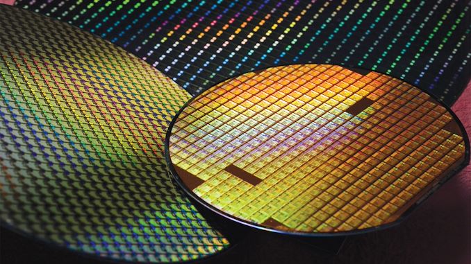
In addition to revealing its roadmap and plans concerning its current leading-edge process technologies, TSMC also shared progress of its N2 node as part of its Symposiums 2024. The company's first 2nm-class fabrication node, and predominantly featuring gate-all-around transistors, according to TSMC N2 has almost achieved its target performance and yield goals, which places it on track to enter high-volume manufacturing in the second half of 2025.
TSMC states that 'N2 development is well on track and N2P is next.' In particular, gate-all-around nanosheet devices currently achieve over 90% of their expected performance, whereas yields of 256 Mb SRAM (32 MB) devices already exceeds 80%, depending on the batch. All of this for a node that is over a year away from mass production.
Meanwhile, average yield of a 256 Mb SRAM was around 70% as of March, 2024, up from around 35% in April, 2023. Device performance has also been improving with higher frequencies being achieved while keeping power consumption in check.
Chip designer interest towards TSMC's first 2nm-class gate-all-around nanosheet transistor-based technology is significant, too. The number of new tape-outs (NTOs) in the first year of N2 is over two-times higher than it was for N5. Though with that said, given TSMC's close working relationship with a handful of high-volume vendors – most notably Appe – NTOs can be a very misleading figure since the first year of a new node at TSMC is capacity constrained, and consequently the bulk of that capacity goes to TSMC's priority partners.
Meanwhile, there were considerably more N5 tapeouts in its second year (some where N5P, of course) and N2 promises to have 2.6X more NTOs in its second year. So the node indeed looks quite promising. In fact, based on TSMC's slides (which we're unfortunately not able to republish), N2 is more popular than N3 in terms of NTOs both in the first and the second years of existence.
When it comes to the second year of N2, in the second half of 2026 TSMC plans to roll out its N2P technology, which promises additional performance and power benefits. N2P is expected to improve frequency by 15% - 20%, reduce power consumption by 30% - 40%, and increase chip density by over 1.15 times compared to N3E, significant benefits to move to all-new GAA nanosheet transistors.
Finally, for those companies that need the best in performance, power, and density, TSMC is poised to offer their A16 process in 2026. That node will also bring in backside power delivery, which will add costs, but is expected to greatly improve performance efficiency and scaling.
Lexar ARMOR 700 Portable SSD Review: Power-Efficient 2 GBps in an IP66 Package
Published: May 30nd 2024 8:00am on AnandTech
Lexar has a long history of serving the flash-based consumer storage market in the form of SSDs, memory cards, and USB flash drives. After having started out as a Micron brand, the company was acquired by Longsys which has diversified its product lineup with regular introduction of new products. Recently, the company announced a number of portable SSDs targeting different market segments. The Lexar ARMOR 700 Portable SSD makes its entry as the new flagship in the 20 Gbps PSSD segment.
Despite its flagship positioning and rugged nature, the ARMOR 700 is reasonably priced thanks to the use of a native USB flash controller - the Silicon Motion SM2320. Similar to the SL500, the product uses YMTC 3D TLC NAND (compared to the usual Micron or BiCS NAND that we have seen in SM2320-based PSSDs from other vendors). Read on for a detailed look at the ARMOR 700, including an analysis of its internals and evaluation of its performance consistency, power consumption, and thermal profile.
Arm Unveils 2024 CPU Core Designs, Cortex X925, A725 and A520: Arm v9.2 Redefined For 3nm
Published: May 29nd 2024 11:00am on AnandTech
As the semiconductor industry continues to evolve, Arm stands at the forefront of innovation for its core and IP architecture, especially in the mobile space, by pushing the boundaries of technology to deliver cutting-edge solutions for end users. For 2024, Arm's year-on-year strategic advancements focus on enhancing last year's Armv9.2 architecture with a new twist. Arm has rebranded and re-strategized its efforts by introducing Client Compute Solutions (CSS), the direct successor to last year's Total Compute Solutions (TSC2023) platform.
Arm is also transitioning its latest IP and Cortex core designs, including the largest Cortex X925, the middle Cortex A725, and the refreshed and smaller Cortex A520 to the more advanced 3 nm process technology. Arm promises that the 3 nm process node will deliver unprecedented performance gains compared to last year's designs, power efficiency and scalability improvements, and new front and back-end refinements to its Cortex series of cores. Arms' new solutions look to power the next-generation mobile and AI applications as Arm, along with its complete AArch64 64-bit instruction execution and approach to solutions geared towards mobile and notebooks, look set to redefine end users' expectations within the Android and Windows on Arm products.
Rapidus Adds Chip Packaging Services to Plans for $32 Billion 2nm Fab
Published: May 24nd 2024 4:00am on AnandTech
To say that the global foundry market is booming right now would be an understatement. Demand for leading-edge process technologies driven by AI and HPC applications is unprecedented, and with Intel joining the contract chipmaking game, this market segment is once again becoming rather competitive as well. Yet, this is exactly the market segment that Rapidus, a foundry startup backed by the Japanese government and several major Japanese companies, is going to enter in 2027, when its first fab comes online, just a few years from now.
In a fresh update on the status of bringing up the company's first leading-edge fab, Rapidus has revealed that they are intending to get in to the chip packaging game as well. Once complete, the ¥5 trillion ($32 billion) fab will be offering both chip lithography on a 2nm node, as well as packaging services for chips produced within the facility – a notable distinction in an industry where, even if packaging isn't outsourced entirely (OSAT), it's still normally handled at dedicated facilities.
Ultimately, while the company wants to serve the same clients as TSMC, Samsung, and Intel Foundry, the firm plans to do things almost completely differently than its competitors in a bid to speed up chipmaking from finishing design to getting a working chip out of the fab.
"We are very proud of being Japanese," said Henri Richard, general manager and president of Rapidus's subsidiary in the U.S. "[…] I know that some people may be looking at this thinking [that] Japan is known for quality, attention to detail, but not necessarily for speed, or flexibility. But I will tell you that Atsuyoshi Koike (the head of Rapidus) is a very special executive. That is, he has all the quality of Japan, with a lot of American thinking. So he is quite a unique guy, and certainly extraordinarily focused on creating a company that will be extremely flexible and extremely quick on its feet."
2nm Only, At FirstPerhaps the most significant difference between Rapidus and traditional foundries is that the company will offer only leading-edge manufacturing technologies to its clients: 2 nm in 2027 (phase 1) and then 1.4 nm in the future (phase 2). This is a stark contrast with other contract fabs, including Intel, which tend to offer their customers a full range of fabrication processes to land more clients and produce more chips. Apparently, Rapidus hopes that that there will be enough Japanese and American chip developers that are inclined to use its 2 nm fabrication process to produce their designs. With that said, the number of chip designers that are using the most advanced production node at any given time is relatively small – limited to large firms who need first-mover advantage and have the margins to justify taking the risk – so it remains to be seen whether Rapidus's business model becomes successful. The company believes it will, since the market of chips made on advanced nodes is growing rapidly.
"Until recently IDC was giving a an estimation of the 2nm and below market as about $80 billion and I think we are going to see soon a revision of the potential to $150 billion," said Richard. "[…] TSMC is the 800 pound gorilla in the space. Samsung is there and Intel is going to enter that space. But the market growth is so significant and the demand is so high, that it does not take a lot of market share for Rapidus to be successful. One of the things that gives me great comfort is that when I talk to our EDA partners, when I talk to our potential clients, it is obvious that the entire industry is looking for alternative supply from a fully independent foundry. There is a place for Samsung in this industry, there is a place for Intel in this industry, the industry is currently owned by TSMC. But another totally independent foundry is more than welcome by all of the ecosystem partners and by the customers. So, I feel really, really good about Rapidus's positioning."
Speaking of advanced process technologies, it is notable that Rapidus does not plan to use ASML's High-NA Twinscan EXE lithography scanners for 2 nm production. Instead, Rapidus is sticking to ASML's proven Low-NA scanners, which will reduce costs of Rapidus's fab, though it will entail usage of EUV double patterning, which brings up costs and lengthens the production cycle in other ways. Even with those trade-offs, SemiAnalysis analysts believe that given the cost of High-NA EUV litho tools and halved imaging field, Low-NA double patterning could be more economically viable.
"We think we are absolutely comfortable with the current [Low-NA EUV] solution for 2nm, but we might consider a different solution at 1.4 nm," said Richard.
For now, only Intel plans to use High-NA tools to make chips on its 14A (1.4 nm-class) fabrication process sometimes in the middle of the decade. TSMC and Samsung Foundry look to be more cautious, so Rapidus is not alone with its attitude towards High-NA EUV tools.
Advanced Packaging at a Leading-Edge FabIn addition to advanced process technologies, high-end chip designers (such as those used for AI and HPC applications) also need advanced packaging technologies (e.g., for HBM integration) and Rapidus is ready to offer them as well. What sets the company apart from its industry peers is that it plans to build and package chips in the same fab.
"We intend to have the backend capability in Hokkaido [semiconductor fab] as a differentiator," Richard said. "We have the benefit of starting from scratch and be able to build probably the first fully integrated front end back end semiconductor fab in the industry, I think. Others will retrofit and modify their existing capacity, but we have a clean sheet of paper and part of the secret sauce that Koike son is bringing to Rapidus are some very interesting ideas on how to integrate both front end and back end amongst others."
Intel, Samsung, and TSMC have separate facilities for chip manufacturing and packaging, as even the most sophisticated packaging methods involving silicon interposers (which are essentially large chips) don't match the complexity of modern processors. The tools that are used to build silicon interposers and equipment used to make full logic chips are vastly different, so installing them into the same cleanroom generally makes little sense as they do not complement each other very well.
On the other hand, transporting wafers from one site to another is a time consuming and risky endeavor, so integrating everything into one campus could make sense as it greatly simplifies supply chain.
"We are going to re reinvent the way, chip design, front end and the back end are working together toward the completion of a project," Richard said. […] The whole idea is we can do it fast, with high quality, high yield, and with a very short cycle time."
MSI Teases Z790 Project Zero Plus Motherboard With CAMM2 Memory Support
Published: May 24nd 2024 8:00am on AnandTech
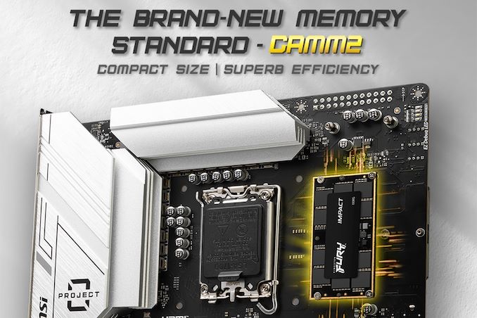
MSI on Thursday published the first image of a new desktop motherboard that supports the innovative DDR5 compression attached memory module (CAMM2). DDR5 CAMM2 modules are designed to improve upon the SO-DIMM form factor used for laptops, alleviating some of the high-speed signaling and capacity limitations of SO-DIMMs while also shaving down on the volume of space required. And while we're eagerly awaiting to see CAMM2 show up in more laptops, its introduction in a PC motherboard comes as a bit of a surprise, since PCs aren't nearly as space-constrained.
MSI's Z790 Project Zero Plus motherboard, which supports Intel's latest 14th Generation Core processors, is to a large degree a proof-of-concept product that is showcasing several new technologies and atypical configuration options. Key among these, of course, is the CAMM2 connector. The single connector supports a 128-bit DDR5 memory bus, allowing for a system to be fully populated with RAM with just a single, horizontally-mounted CAMM2 module. And in terms of design, the Zero Plus also features backside power connectors for improved cable management.

CAMM2 is designed to replace traditional modules in an SO-DIMM form-factor and is meant to occupy up to 64% less space than two DDR5 SO-DIMMs. In addition, CAMM2 greatly optimizes signal and power traces inside the motherboard, primarily by ensuring all memory trace lengths are identical, reducing some of the signaling penalties that normally come from supporting multiple SO-DIMM slots in a system. With DDR5 being particularly sensitive here – to the point where 2 DIMM Per Channel (2DPC) configurations take a max frequency hit even on desktop systems – CAMM2 modules are expected to simplify and, to a degree, improve laptop designs to better match DDR5's limitations.
Though whether CAMM2 sees widespread adoption remains to be seen. Unlike it's LPDDR5X counterpart, LPCAMM2, DDR5 CAMM2 hasn't attracted the same interest from laptop vendors quite yet, in large part because it doesn't introduce any new functionality (e.g. socketed LPDDR5X).
Meanwhile CAMM2 in ATX desktops is all but unexplored right now, which is why we're seeing experimental products like MSI's motherboard. The space savings alone aren't as important in desktops due to their size – though CAMM2 does cut down on Z-height, keeping memory away from CPU coolers. But PC makers will be looking at other factors such as inventory, as equipping desktop boards with CAMM2 connectors would allow them to use the same memory modules in both laptops and desktops. And longer term there is the question of whether CAMM2 can deliver tangible signaling benefits over traditional DIMMs.
MSI plans to showcase its Z790 Project Zero Plus platform at Computex, alongside memory partner Kingston. The latter will be at the show to demonstrate its Fury Impact CAMM2 memory module, which is one of the first DDR5 CAMM2 modules to be announced.
ASUS NUC14RVHv7 and ASRock Industrial NUC BOX-155H Review: Meteor Lake Brings Accelerated AI to UCFF PCs
Published: May 23nd 2024 8:00am on AnandTech
Intel's Meteor Lake series of processors has had a drawn-out launch since its details were officially presented in September 2023. The series marks Intel's foray into the consumer market with a tile-based chiplet configuration held together with Foveros packaging. Similar to Tiger Lake, the focus of Meteor Lake has primarily been on the mobile market - ultraportables and notebooks. However, this has not prevented Intel and its partners from introducing it as a follow-up to Raptor Lake-P and Raptor Lake-H in the SFF / UCFF desktop market.
ASRock Industrial has consistently been the first to market with ultra-compact form-factor motherboards and mini-PCs, with product announcements coinciding with Intel's launch of its latest and greatest mobile processors. Meteor Lake has not been any different, with the NUC(S) Ultra 100 BOX series launching towards the end of Q4 2023. In the meanwhile, Intel's NUC business unit was purchased by ASUS and had its first major product announcement in the form of the Meteor Lake-based Revel Canyon NUCs at the 2024 CES.
The flagship NUC Ultra 100 BOX system is the NUC BOX-155H based on the Intel Core Ultra 7 155H. The Revel Canyon NUC lineup includes a model based on the Core Ultra 7 165H with vPro capabilities, with its claim to fame being the ability to hit 5 GHz on the performance cores. Read on for a detailed look at the features and performance profile of the ASRock Industrial NUC BOX-155H and the ASUS NUC14RVHv7. The analysis also helps in establishing the potential and benefits of Meteor Lake for the UCFF desktop market over its predecessors and the competition.
TSMC's Roadmap at a Glance: N3X, N2P, A16 Coming in 2025/2026
Published: May 22nd 2024 5:30am on AnandTech

As announced last week by TSMC, later this year the company is set to start high-volume manufacturing on its N3P fabrication process, and this will be the company's most advanced node for a while. Next year things will get a bit more interesting as TSMC will have two process technologies that could actually compete against each other when they enter high-volume manufacturing (HVM) in the second half of 2025.
Advertised PPA Improvements of New Process Technologies Data announced during conference calls, events, press briefings and press releases Compiled by AnandTech TSMC N3 vs N5 N3E vs N5 N3P vs N3E N3X vs N3P N2 vs N3E N2P vs N3E N2P vs N2 A16 vs N2P Power -25% -30% -34% -5% -10% -7%*** -25% -30% -30% -40% -5% -10% -15% -20% Performance +10% +15% +18% +5% +5% Fmax @1.2V** +10% +15% +15% +20% +5 +10% +8% +10% Density* ? 1.3x 1.04x 1.10x*** 1.15x 1.15x ? 1.07x 1.10x HVM Q4 2022 Q4 2023 H2 2024 H2 2025 H2 2025 H2 2026 H2 2026 H2 2026*Chip density published by TSMC reflects 'mixed' chip density consisting of 50% logic, 30% SRAM, and 20% analog. **At the same area. ***At the same speed.
The production nodes are N3X (3nm-class, extreme performance-focused) as well as N2 (2nm-class). TSMC says that when compared to N3P, chips made on N3X can either lower power consumption by 7% at the same frequency by lowering Vdd from 1.0V to 0.9V, increase performance by 5% at the same area, or increase transistor density by around 10% at the same frequency. Meanwhile, the key advantage of N3X compared to predecessors is its maximum voltage of 1.2V, which is important for ultra-high-performance applications, such as desktop or datacenter GPUs.
TSMC's N2 will be TSMC's first production node to use gate-all-around (GAA) nanosheet transistors and this will significantly enhance its performance, power, and area (PPA) characteristics. When compared to N3E, semiconductors produced on N3 can cut their power consumption by 25% - 30% (at the same transistor count and frequency), increase their performance by 10% - 15% (at the same transistor count and power), and increase transistor density by 15% (at the same speed and power).
While N2 will certainly be TSMC's undisputed champ when it comes to power consumption and transistor density, N3X could possibly challenge it when it comes to performance, especially at high voltages. For many customers N3X will also have a benefit of using proven FinFET transistors, so N2 will not be automatically the best of TSMC's nodes in the second half of 2025.
2026: N2P and A16In the following year TSMC will again offer two nodes that are set to target generally similar smartphone and high-performance computing applications: N2P (performance-enhanced 2nm-class) and A16 (1.6nm-class with backside power delivery).
N2P is expected to deliver a 5% - 10% lower power (at the same speed and transistor count) or a 5% - 10% higher performance (at the same power and transistor count) compared to the original N2. Meanwhile, A16 is set to offer an up to 20% lower power (at the same speed and transistors), up to 10% higher performance (at the same power and transistors), and up to 10% higher transistor density compared to N2P.
Keeping in mind that A16 features enhanced backside power delivery network, it will likely be the node of choice for performance-minded chip designers. But of course, it will be more expensive to use A16 because of the backside power delivery, which requires additional process steps.
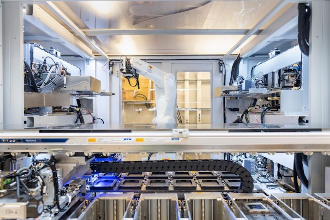
TSMC Offers a Peek at 'Global Gigafab' Process Replication Program
Published: May 22nd 2024 3:00am on AnandTech
At its European Technology Symposium last week TSMC revealed some of the details about its Global Gigafab Manufacturing program, the company's strategy to replicate its manufacturing processes across its multiple gigafab sites.
The need for large-scale multi-national fabs to have a process in place to replicate their facilities is well-documented at this point. As scaling-up at at the gigafab size means scaling-out instead, chip makers need to be able to quickly get new and updated manufacturing processes ported to other facilities in order to hit their necessary throughput – and to avoid a multi-quarter bottlenecks that come from having to freshly-tune a fab.
Intel, for their part, has a well-known Copy Exactly program, which is one of the company's major competitive advantages, allowing it to share process recipes across its fabs around the world to maximize yields and reduce performance variability. Meanwhile, as Taiwan Semiconductor Manufacturing Co. is building additional capacity in different parts of the world, it has reached the point where it needs a similar program in order to quickly maximize its yields and productivity at its new fabs in Japan and the U.S. And in some respects, TSMC's program goes even further than Intel's, with an additional focus on sustainability and social responsibility.
"As mentioned at last year's symposium, [Global Gigafab manufacturing] is a powerful global manufacturing and management platform," said Y.L. Wang, Vice President of Fab Operations TSMC. "We realise one fab management to ensure our Gigafab to achieve consistent operation efficiency as well as production quality on a global scale. Moreover, we also pursue sustainability across our global footprint covering green manufacturing, global talent development, supply chain localization, as well as social responsibility."
TSMC's Global GigaFab Manufacturing Data by TSMC (Compiled by AnandTech) Manufacturing Excellence Sustainability Global One Fab Manufacturing Green Manufacturing ML-based Process Control Global Talent Development Manufacturing Agility and Quality Supply Chain Localization Maximum Productivity Social ResponsibilityWhen it comes to improvements of process technology, there are two main mechanisms: the continuous process improvements (CPI) to improve yields, as well as statistical process control (SPC) reduce performance variations. To do so, the company has multiple internal techniques that rely on machine learning-based process control, constant quality measuring, and various productivity improving methods. With Global Gigafab manufacturing TSMC can use CPI and SPC to improve yields and performance on the global scale by sharing knowledge between different sites.
"When we port a technology from Taiwan to Arizona, the fab set up, the process control system, everything is actually a copy from Taiwan," said Kevin Zhang, Senior Vice President, Business Development and Overseas Operations Office, and Deputy Co-COO at TSMC.
TSMC yet has to start making chips at its fabs in Germany, Japan, and the United States, so it remains to be seen how fast the foundry will increase yields to Taiwanese levels at its Fab 23 (in Kumamoto, Japan) and Fab 21 (in Arizona) when they begin operations in 2024 and 2025, but with Global Gigafab Manufacturing program in place, this is likely set to happen rather sooner than later.
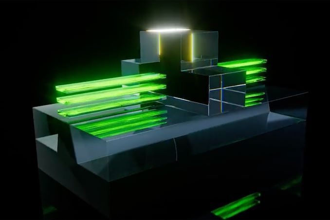
TSMC to Expand CoWoS Capacity by 60% Yearly Through 2026
Published: May 21nd 2024 11:00am on AnandTech
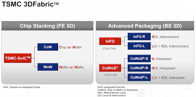
Customer demand for AI and HPC processors is driving a much greater use of advanced packaging technologies, particularly TSMC's chip-on-wafer-on-substrate (CoWoS) services. As things stand, TSMC is just barely meeting the current demand for this packaging method – never mind future demand – which is why last year the company announced plans to more than double CoWoS capacity by the end of 2024. But as it turns out, just doubling capacity once won't be enough, and the world's largest contract maker of chips is going to have to keep scaling up at a rapid pace.
At its European Technology Symposium last week TSMC announced plans to expand CoWoS capacity at a compound annual growth rate (CAGR) of over 60% till at least 2026. As a result, TSMC's CoWoS capacity will more than quadruple from 2023 levels by the end of that period. And keeping in mind that TSMC is prepping additional versions of CoWoS (namely CoWoS-L) that will enable building system-in-packages (SiPs) of up to eight reticle sizes, increasing CoWoS capacity by four-fold in three years may still not be enough. The good news is that the various third-party off-site assembly and testing (OSAT) providers are also expanding their CoWoS-like capacity, so the demand for advanced packing isn't a problem that TSMC is facing (or resolving) on their own.
And CoWoS isn't the only advanced packaging technology line whose capacity TSMC is looking to rapidly expand. The company also has its system-on-integrated chips (SoIC) 3D stacking technology which adoption is poised to grow in the coming years. To meet demand for its SoIC packaging methods TSMC will expand SoIC capacity at a 100% compound annual growth rate by the end of 2026. As a result, SoIC capacity will grow by eight-fold from 2023 levels by late 2026.
Overall, TSMC itself expects leading-edge SiPs for demanding applications like AI and HPC will adopt both CoWoS and SoIC 3D stacking technologies in the coming years, which is why it needs to increase capacity for both methods to be able to build those highly-complex processors.
One More EPYC: AMD Launches Entry-Level Zen 4-based EPYC 4004 Series
Published: May 21nd 2024 9:00am on AnandTech

Ever since AMD re-emerged as a major competitor within the x86 CPU scene, one of AMD’s top priorities has been to win over customers in the highly lucrative and profitable server market. It’s a strategy that’s paid off well for AMD, as while they’re still the minority player in the space, they’ve continued to whittle away at what was once Intel’s absolute control over the market, slowly converting more and more customers over to the EPYC ecosystem.
Now as the Zen 4 CPU architecture approaches its second birthday, AMD is launching one final line of EPYC chips, taking aim at yet another Xeon market segment. This time it’s all about the entry-level 1P server market – small scale, budget-conscientious users who only need a handful of CPU cores – which AMD is addressing with their new EPYC 4004 series processors.
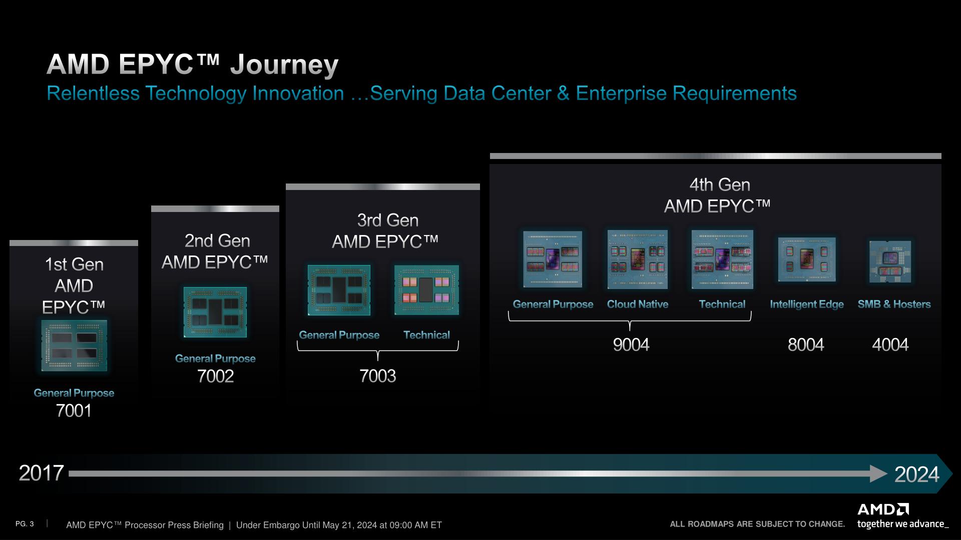
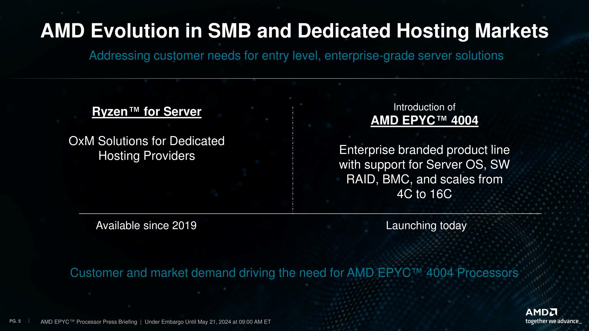
Within AMD’s various product stacks, the new EPYC 4004 family essentially replaces Ryzen chips for use in servers. Ryzen for servers was never a dedicated product lineup within AMD, but none the less it has been a product segment within the company since 2019, with AMD aiming it at smaller-scale hosting providers who opted to use racks of consumer-scale hardware, rather than going the high-density route with high core count EPYC processors.
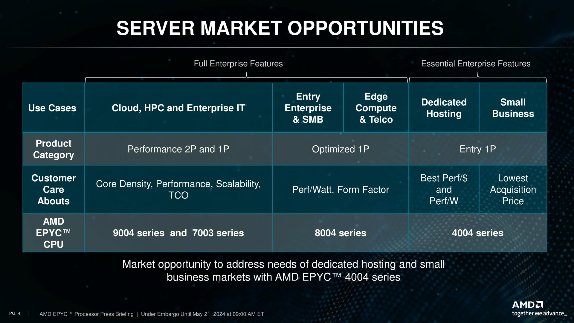
With the upgrade to EPYC status, that hardware ecosystem is being re-deployed as a proper lineup with dedicated chips, and a handful of additional features befitting an EPYC chip. Consequently, AMD is also expanding the scope of the market segments they’re targeting by a hair, roping in small business (SMB) users, whom AMD wasn’t previously chasing. Though regardless of the name on the market segment, the end result is that AMD is carving out a budget-priced series of EPYC chips with 4 to 16 cores based on their consumer platforms.
Underlying the new EPYC 4004 series is AMD’s tried and true AM5 platform and Raphael processors, which we know better as the Ryzen 7000 series. Their new EPYC counterparts are an 8 chip stack that is comprised almost entirely of rebranded Ryzen 7000 SKUs, with all the same core counts, clockspeeds, and TDPs as their counterparts. The sole exception here being the very cheapest chip of the bunch, the 4 core 4124P.
AMD EPYC 4004 Processors AnandTech Core/ Thread Base Freq 1T Freq L3 Cache PCIe Memory TDP (W) Price (1KU) Ryzen Version 4584PX 16 32 4200 5700 128MB (3D) 28 x 5.0 2 x DDR5-5200 UDIMM 120 $699 7950X3D 4484PX 12 24 4400 5600 128MB (3D) 120 $599 7990X3D 4564P 16 32 4500 5700 64MB 170 $699 7950X 4464P 12 24 3700 5400 64MB 65 $429 7900 4364P 8 16 4500 5400 32MB 105 $399 7700X 4344P 8 16 3800 5300 32MB 65 $329 7700 4244P 6 12 3800 5100 32MB 65 $229 7600 4124P 4 8 3800 5100 16MB 65 $149 NewSince these are all based on AMD’s consumer discrete CPUs, the underlying architecture in all of these chips is Zen 4 throughout. So despite being positioned below the EPYC 8004 Siena series, you won’t find any Zen 4c CPU cores here; everything is full-fat Zen 4 CCDs. Which means that while there are relatively few cores overall (for an EPYC processor), they are all high-performing cores, with nothing turboing lower than 5.1GHz.
Notably here, AMD is mixing in some of their 3D V-Cache chip SKUs as well, which are signified with the “PX” suffix. Based on the 7950X3D and 7900X3D respectively, both of these chips have 1 CCD with V-Cache stacked on top of them, affording the chip a total of 128MB of L3 cache. The remaining 6 SKUs all get the “P” suffix – indicating they’re 1 socket processors – and come with TDPs ranging from 65 Watts to 170 Watts.
This does mean that, by EPYC server standards, the 4004 series is not particularly energy efficient. This is a lineup that is intended to be cost-effective first and foremost. Instead, energy efficiency remains the domain of the EPYC 8004, with its modestly-clocked many-core Zen4c designs.
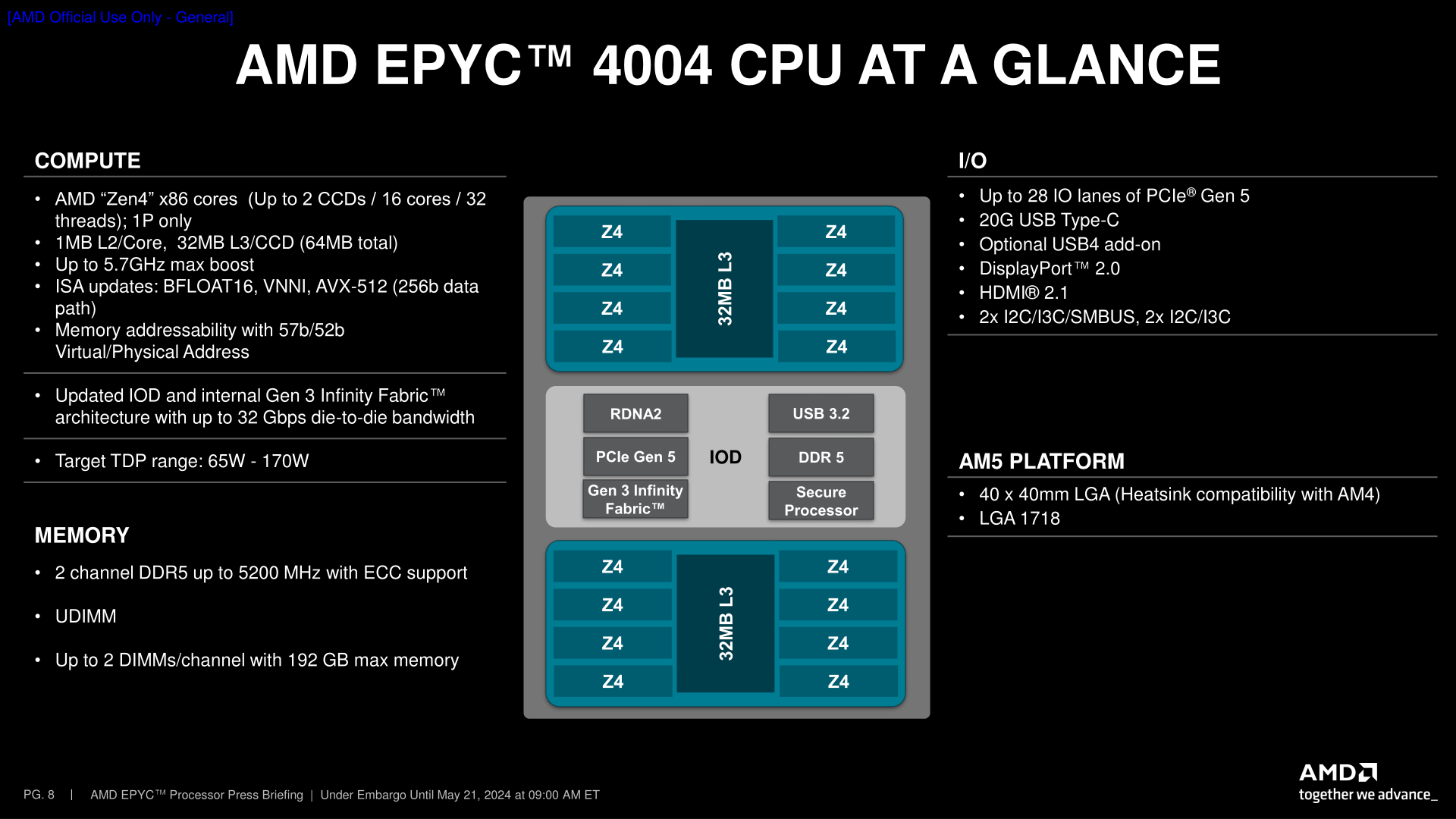
The reuse of Zen 4/AM5 means that the EPYC 4004 series comes with all of the features we’ve come to expect from the platform, including 28 lanes of PCIe 5.0, 2 channels (128-bits) of DDR5 memory at speeds up to DDR5-5200, and even integrated graphics. Since this is a server part, ECC is officially supported on the chips – though do note that like the Ryzen Pro workstation chips, this is UDIMM-only; registered DIMMs (RDIMMs) are not supported.
AMD isn’t disclosing the chipset being paired with the EPYC 4004 processors, and while it’s undoubtedly going to be AMD’s favorite ASMedia-designed I/O chipset, it’s interesting to note that it’s at the motherboard level where the new EPYC platform’s real server credentials are at. Separating itself from rank-and-file Ryzens, the EPYC 4004 platform is getting several additional enterprise features, including baseboard management controller (BMC) support, software RAID (RAIDXpert2 for Server), and official server OS support. To be sure, this is still a fraction of the features found in a high-end enterprise solution like the EPYC 9004/8004 series, but it’s some additional functionality befitting of a platform meant to be used in servers.
AMD’s new chips, in turn, are designed to compete against Intel’s entry-level Xeon-E family. Itself a redress of consumer hardware (Raptor Lake), the Xeon-E family is a P-core only chip lineup, with Intel offering SKUs with 4, 6, or 8 CPU cores. This leaves the EPYC 4004 family somewhat uniquely positioned compared to the Xeon-E family, as Intel doesn’t have anything that’s a true counterpart to AMD’s 12 and 16 core chips; after Xeon-E comes the far more capable (and expensive) Xeon-w family. So part of AMD’s strategy with the EPYC 4004 family is to serve a niche that Intel does not.
(As a side bonus, AMD’s core counts also end up playing well with Windows Server 2022 licensing. The Standard license covers up to 16 cores, so a top-end EPYC 4004 chip lets server owners max out their license, amortizing the software cost over more cores)
With regards to performance, Raptor Lake versus Zen 4 is largely settled by now. So I won’t spend too much time on AMD’s (many) benchmark slides. But suffice it to say, with a significant core count advantage, AMD can deliver an equally significant performance advantage in highly multi-threaded workloads (though in that scenario, it does come with a similar spike in power consumption compared to the 95 Watt Intel chips).
Wrapping things up, AMD is launching the new EPYC 4004 product stack immediately. With many of AMD’s regular server partners already signed up – and the core hardware readily available – there won’t be much of a ramp-up period to speak of.
Gallery: EPYC 4004 Press Deck


